


+86 13603063656
ENIG (Electroless Nickel Immersion Gold), also known as “nickel-gold plating” or “immersion gold PCB,” is a critical surface finishing process for printed circuit boards (PCBs). Widely adopted in high-end electronics—including smartphones, BGA carriers, and COB (Chip-On-Board) modules—ENIG combines excellent solderability, corrosion resistance, and wire bonding capability, making it a go-to choice for precision electronics. In this guide, we dive deep into ENIG’s technology, process flow, pros/cons, and why Jerico Multilayer PCB supplier stands out as a trusted partner for ENIG manufacturing.
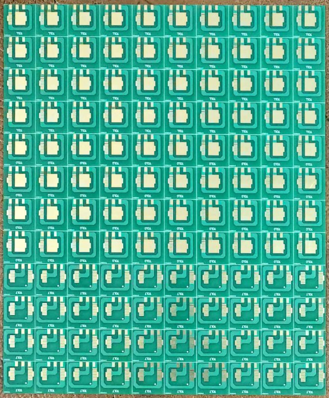
ENIG PCB Surface Treatment
ENIG is a two-layer metal coating (nickel + gold) applied to copper pads via chemical plating, eliminating the need for electrolytic current. Unlike electroplated nickel-gold, ENIG skips wire bonding for each pad, simplifying production and reducing costs by up to 30%. Its core structure includes:
The ENIG process involves 10+ steps, each critical to ensuring coating uniformity and performance:
Pro Tip: Over-etching during micro-etching can create deep grooves, risking gold layer penetration and “black pad” defects. Jerico Multilayer PCB uses automated micro-etching controls to minimize this risk.
Industry Case: Jerico Multilayer PCB’s ENIG boards are used in 5G smartphones, where 0.4mm-pitch BGA components require zero solder joint failures—ENIG’s precision delivers.
Despite its benefits, ENIG faces two key issues:
Caused by excessive nickel oxidation during gold immersion, black pads weaken solder joints. Solution:
Gold’s price volatility makes ENIG pricier than organic solderability preservatives (OSP). Mitigation:
Jerico Multilayer PCB is a global leader in ENIG manufacturing, offering:
Q1: Is ENIG suitable for high-temperature applications?
A: Yes. ENIG withstands up to 280°C for short periods (e.g., wave soldering) and 3+ reflows at 260°C, making it ideal for automotive and industrial electronics.
Q2: How does ENIG compare to OSP in cost?
A: ENIG is 2-3x pricier than OSP due to gold usage, but its reworkability and reliability justify the cost for mission-critical applications.
Q3: Can ENIG boards be reworked?
A: Yes. ENIG supports soldering/desoldering up to 3 times without significant coating degradation—critical for prototype iterations.
Q4: What’s the ideal gold thickness for BGA pads?
A: 0.05-0.1μm balances cost and reliability. For COB or high-vibration environments, increase to 0.15-0.3μm.
Q5: How long does ENIG last in storage?
A: Properly stored (dry, <25°C, <60% RH), ENIG boards remain solderable for 12+ months. Jerico Multilayer PCB provides 6-month shelf-life guarantees with proper packaging.
ENIG remains a cornerstone of high-reliability PCB manufacturing, offering unmatched solderability and corrosion resistance. By partnering with Jerico Multilayer PCB—experts in ENIG process optimization—you can mitigate common defects (e.g., black pads) and deliver boards that meet the demands of 5G, AIoT, and automotive electronics.


Connect to a Jerico Multilayer PCB engineer to support your project!
Request A Quote


 Quote
Quote