


+86 13603063656
A double-sided PCB (printed circuit board) is a type of circuit board that has conductive traces and components on both sides of its substrate. It’s a common choice for a variety of electronic applications, as it allows for higher density, better performance, and more efficient use of board space. Whether you’re working in consumer electronics, automotive systems, or power electronics, understanding the advantages and applications of double-sided PCBs is essential for designing compact, reliable, and high-performance products.

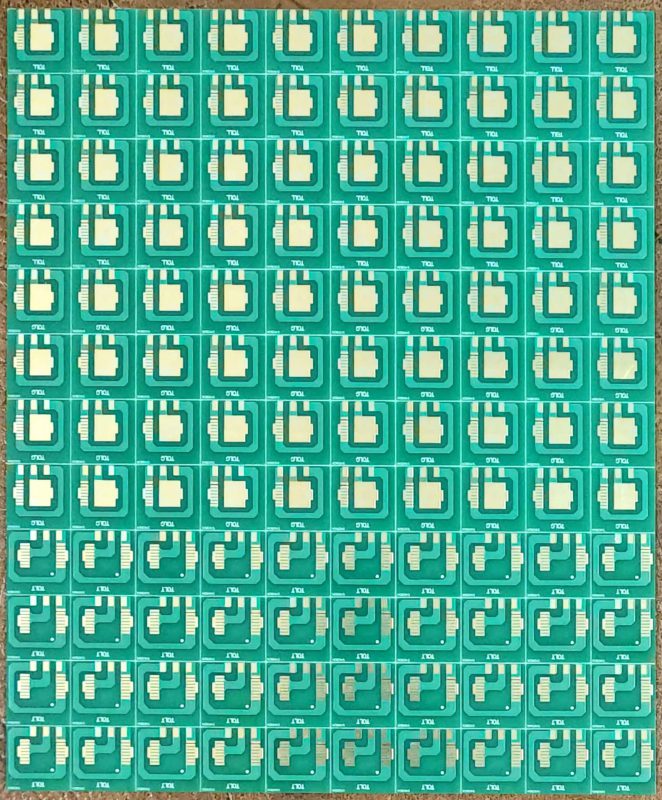
Double-Sided PCB Board
A double-sided PCB is a circuit board that has conductive traces on both its top and bottom surfaces. Unlike a single-sided PCB, where components and traces are only placed on one side, a double-sided PCB allows for more complex circuits to be built on a single board, increasing the design’s capacity without enlarging the footprint.
But here’s the kicker — this added flexibility enables engineers to design circuits with more connections and less space, making double-sided PCBs the ideal choice for compact devices that require high functionality, such as smartphones, medical devices, and automotive electronics.
The design of a double-sided PCB includes:
Copper Layers: Copper traces are applied to both sides of the substrate.
Vias: These are small holes that connect the copper layers, allowing electrical signals to travel between the top and bottom layers.
Soldering Pads: These are located on both sides, allowing components to be mounted on either surface.
The layout is often more complex than single-sided PCBs, requiring careful planning to optimize space and ensure the signals and power flow correctly.
| Feature | Single-Sided PCB | Double-Sided PCB |
|---|---|---|
| Copper Layers | One side only | Both sides |
| Component Placement | One side only | Both sides |
| Complexity | Low | High |
| Applications | Basic electronics | Compact, high-performance electronics |
| Cost | Lower | Higher |
Double-sided PCBs offer a variety of advantages that make them ideal for certain applications. One of the key benefits is the ability to place components on both sides of the board, which optimizes space and allows for more intricate designs. But here’s the kicker — this space efficiency enables the creation of smaller, more compact electronic devices without sacrificing functionality.
Advantages of using double-sided PCBs include:
Higher Component Density: The ability to place components on both sides increases the overall density, making them suitable for applications where space is limited.
Improved Performance: Double-sided PCBs allow for shorter traces, which means faster signal transmission and less signal degradation.
Cost-Effectiveness for Medium Complexity Designs: For designs with moderate complexity, double-sided PCBs can be more cost-effective than using a multilayer PCB, especially for lower-volume production.
Thermal Efficiency: By spreading out components across both sides of the board, double-sided PCBs can help with heat dissipation, preventing overheating.
| Advantage | Description |
|---|---|
| Higher Component Density | Utilizes both sides for more components |
| Improved Performance | Shorter signal paths reduce loss and improve speed |
| Cost Efficiency | More affordable for moderate complexity than multilayer |
| Thermal Efficiency | Enhanced heat dissipation due to component spacing |
Manufacturing double-sided PCBs involves several critical steps. These steps ensure that both sides of the board are properly populated with conductive traces, components, and vias to allow electrical signals to flow seamlessly between the two surfaces.
Ready for the good part? The process for double-sided PCBs is more involved than single-sided boards but offers the flexibility needed for more complex designs. Here’s how it works:
Step 1: Copper Cladding: A layer of copper is applied to both sides of a non-conductive substrate.
Step 2: Drilling: Holes are drilled into the board to allow vias to connect the two sides of the PCB.
Step 3: Etching: The unwanted copper is removed, leaving only the traces on both sides of the PCB.
Step 4: Component Mounting: Components are soldered onto both sides of the PCB, using techniques like wave soldering, hand soldering, or reflow soldering.
Step 5: Testing: The PCB undergoes testing for electrical performance, ensuring that all components are working as expected.
The precision and quality of each step in the manufacturing process are crucial to ensuring the final product performs reliably.
| Step | Description |
|---|---|
| Copper Cladding | Applying copper to both sides of the substrate |
| Drilling | Creating holes for vias to connect the two sides |
| Etching | Removing excess copper to form traces |
| Component Mounting | Soldering components onto both sides of the board |
| Testing | Verifying electrical connectivity and functionality |
Double-sided PCBs are ideal when you need a compact design with higher density and more complex routing than a single-sided PCB can offer. They’re used in a variety of industries, including consumer electronics, automotive systems, and telecommunications.
This is where it gets interesting — a double-sided PCB isn’t always the best choice. For very simple circuits, a single-sided PCB may be more cost-effective, and for extremely complex designs, a multilayer PCB may be necessary. The key is understanding when a double-sided PCB will meet your needs without overcomplicating the design.
Use a double-sided PCB when:
You need more components on the board than a single-sided design allows.
You require efficient use of board space without increasing the board size.
You’re designing for medium-complexity devices like mobile phones, power supplies, or automotive electronics.
| Scenario | Why Double-Sided Works |
|---|---|
| Space-limited design | Maximizes component density within a compact area |
| Moderate complexity | Ideal for applications with multiple components |
| Power electronics | Helps with heat dissipation and efficient routing |
| Consumer electronics | Allows for smaller designs with more features |
Placing components on both sides of a double-sided PCB requires careful planning and specialized techniques. The key to managing this complexity is the use of vias, which are small holes drilled through the board that allow electrical connections to be made between the top and bottom layers.
What’s the real story? Managing the placement of components on both sides requires balancing accessibility, thermal management, and electrical performance. Proper routing and via placement are crucial to ensure the PCB functions optimally without introducing interference or signal degradation.
The process typically involves:
Top-side component placement: Components are placed and soldered on the top layer of the PCB.
Bottom-side component placement: The bottom layer is populated similarly, often requiring careful alignment to avoid conflicts with the top-side components.
Via usage: Vias are strategically placed to route signals between the two sides of the PCB, ensuring proper connections and minimizing interference.
| Placement Area | Key Considerations | Benefits |
|---|---|---|
| Top-side | Ensure components are spaced for heat dissipation | Maximizes space efficiency |
| Bottom-side | Align components to avoid top-side conflicts | Utilizes available space |
| Via Placement | Strategically place vias for electrical integrity | Ensures connection between layers |
Double-sided PCBs are versatile and used across numerous industries. Their ability to handle complex circuits while maintaining a compact form makes them ideal for consumer electronics, automotive systems, medical devices, and more.
Ready for the good part? Double-sided PCBs are especially useful in high-frequency and power-intensive applications, where their design allows for more efficient routing and heat dissipation. Here are some of the most common applications:
Consumer Electronics: Smartphones, tablets, and wearables require compact, high-density PCBs that can support multiple components and maintain performance.
Automotive Systems: Control modules, sensors, and power systems benefit from the reliability and efficiency of double-sided PCBs.
Medical Devices: Diagnostic tools, monitoring systems, and portable health devices all require the reliability and functionality of double-sided PCBs.
| Application | Reason for Use | Examples |
|---|---|---|
| Consumer Electronics | Space-saving design with high density | Smartphones, Tablets, Wearables |
| Automotive Electronics | Compact, reliable circuits for control | Sensors, Power Modules |
| Medical Devices | Durable, high-performance for critical systems | Diagnostic Equipment, Monitors |
| Power Electronics | Efficient power distribution and heat management | Power Supplies, LED Drivers |
Double-sided PCBs offer several benefits in terms of electrical performance. By utilizing both sides of the board, you can create shorter, more direct signal paths, which results in faster signal transmission and less signal degradation.
What’s the real story? This reduction in trace length and routing complexity improves both signal integrity and electrical efficiency. Moreover, double-sided PCBs allow for better power distribution by placing power and ground planes on each layer, ensuring more stable performance.
Advantages include:
Reduced Cross-Talk: Shorter traces reduce interference between circuits.
Lower Impedance: A well-designed double-sided PCB has lower impedance, which improves signal quality.
Better Power Distribution: Dedicated power and ground planes on both sides enhance the PCB’s ability to manage high-current demands.
| Benefit | How It Helps Electrical Performance | Example |
|---|---|---|
| Reduced Cross-Talk | Shorter traces reduce noise and interference | Audio equipment, high-speed circuits |
| Lower Impedance | Ensures higher signal fidelity | Telecommunications, RF systems |
| Improved Power Distribution | Consistent power flow, reduced noise | Power supplies, automotive ECUs |
Designing double-sided PCBs requires a balance between electrical performance, component placement, and manufacturing capabilities. Proper planning and DFM (Design for Manufacturing) guidelines are crucial to avoid errors and ensure the board is both functional and manufacturable.
But here’s the kicker — small design errors in double-sided PCBs can lead to significant problems, like component misalignment or signal interference.
Key design considerations include:
Via Placement: Ensuring vias don’t obstruct components or signal pathways.
Thermal Management: Ensuring adequate spacing and via holes to manage heat dissipation.
Trace Routing: Keeping traces as short and direct as possible to minimize resistance and improve performance.
| Consideration | Impact on Performance | Best Practice |
|---|---|---|
| Via Placement | Affects signal integrity and routing | Minimize via count, keep them on layer edges |
| Thermal Management | Reduces the risk of overheating | Use copper pours for heat dissipation |
| Trace Routing | Affects signal speed and loss | Keep traces as short as possible, use proper width |
Soldering double-sided PCBs presents unique challenges. The need to solder components on both sides requires specialized techniques to ensure both sides are properly soldered without interference.
What’s the real story? The two primary soldering techniques used for double-sided PCBs are wave soldering and reflow soldering. In addition to these, manual soldering is often required for certain components. The key challenge is ensuring that components on both sides of the board are not damaged or misaligned during the soldering process.
| Technique | Best For | Advantages |
|---|---|---|
| Wave Soldering | Through-hole components | Fast, efficient for mass production |
| Reflow Soldering | Surface-mount components | Precision, ideal for fine-pitch components |
| Manual Soldering | Small batch runs or prototypes | Flexibility for complex assemblies |
Testing double sided PCBs ensures that they function properly and meet all relevant standards for electrical performance, thermal stability, and durability.
Ready for the good part? Testing starts with electrical testing to ensure continuity and resistance. Then, visual inspection checks for defects like solder bridges or component misalignment. Finally, more advanced tests, such as X-ray inspection, are performed for internal components like BGAs.
| Test Method | Purpose | Tools Used |
|---|---|---|
| Electrical Testing | Ensure continuity, isolation, and values | Multimeter, ICT |
| Visual Inspection | Check for surface defects | AOI, manual inspection |
| X-Ray Inspection | Detect internal component issues | X-ray machine |
When designing for high-density applications, both double-sided and multilayer PCBs offer distinct advantages. While double-sided boards are ideal for medium-complexity designs, multilayer PCBs are used for high-performance circuits with more layers for routing.
What’s the real story? Double sided PCBs are more cost-effective and easier to manufacture than multilayer designs, but they have limitations in routing complexity and electrical isolation. Multilayer PCBs, on the other hand, provide more robust performance at a higher cost.
| Feature | Double Sided PCB | Multilayer PCB |
|---|---|---|
| Complexity | Moderate | High |
| Cost | Lower | Higher |
| Performance | Suitable for medium complexity | High-frequency, high-speed |
| Manufacturing Time | Short | Longer |
When choosing between single-sided, double-sided, and multilayer PCBs, the cost is a significant factor. Double sided PCBs are generally more expensive than single-sided boards but less costly than multilayer designs.
Ready for the good part? The cost depends on the complexity of the design, the materials used, and the number of layers. Double sided boards offer a sweet spot between cost and performance for medium-complexity applications.
| PCB Type | Cost | Best Use Case |
|---|---|---|
| Single-Sided PCB | Low | Simple, low-density circuits |
| Double Sided PCB | Moderate | Medium-complexity designs |
| Multilayer PCB | High | High-speed, high-frequency circuits |
Designing double sided PCBs requires careful consideration of component placement, trace routing, and the use of vias. Improper design can lead to performance degradation or manufacturing issues.
What’s the real story? The biggest challenge is balancing complexity with manufacturability, especially when working with high-speed or high-power circuits.
| Challenge | Impact | Solution |
|---|---|---|
| Via Placement | Can affect signal integrity | Strategic via placement, minimize number |
| Component Overlap | Can cause misalignment or shorts | Use proper spacing and layer management |
| Heat Management | Can lead to overheating | Use proper copper pours for thermal management |
Double-sided PCBs are increasingly being used in high-performance applications, especially those that require both compact design and high efficiency. They are essential in fields like telecommunications, aerospace, and automotive electronics.
Ready for the good part? Double-sided PCBs provide an efficient and reliable solution for applications requiring dense, fast, and robust circuitry without the need for expensive multilayer designs.
| Industry | Use Case | Benefit |
|---|---|---|
| Telecommunications | Signal processors, routers | Compact design, high-speed performance |
| Aerospace | Flight control systems, sensors | High reliability, reduced weight |
| Automotive | ECU, sensor systems | Cost-effective, efficient routing |
The future of double-sided PCB technology looks bright, with continuous innovations improving their capabilities. As devices get smaller and more powerful, the demand for double-sided PCBs that can handle higher component densities, higher frequencies, and better thermal management will increase.
This is where it gets interesting — ongoing developments in flexible PCBs, 3D printing for PCBs, and AI-driven design tools are pushing the boundaries of what double-sided PCBs can do. Expect to see more widespread use in flexible and wearable electronics in the coming years.
| Trend | Impact | Example Applications |
|---|---|---|
| Flexible PCBs | Lightweight, bendable, compact | Wearables, medical devices |
| 3D Printed PCBs | Custom, rapid prototyping | Consumer electronics, R&D |
| AI-Powered Design | Faster, more accurate design | High-frequency communication devices |
Double sided PCBs have become a crucial part of modern electronics. Offering improved density, electrical performance, and cost-effectiveness compared to single-sided designs, they are used in a wide range of applications, from consumer electronics to aerospace. Understanding the design, manufacturing, and testing processes involved in double-sided PCB production can help you choose the right solution for your project, ensuring optimal performance and reliability.
Q1: What is a double sided PCB?
A double-sided PCB is a type of printed circuit board with conductive layers on both sides, allowing components to be placed and traces routed on both sides for more compact and efficient designs.
Q2: How does double sided PCB design compare to single-sided and multilayer PCBs?
Double-sided PCBs are more complex and costlier than single-sided boards but less expensive than multilayer PCBs. They are suitable for medium-complexity designs.
Q3: What are the advantages of using a double sided PCB?
Double-sided PCBs allow for higher component density, reduced signal path lengths, and better electrical performance, making them ideal for many electronic applications.
Q4: What are the main challenges in designing double sided PCBs?
Key challenges include managing component placement, trace routing, and ensuring proper thermal management, especially when dealing with high-speed or high-power circuits.
Q5: What are the common applications of double sided PCBs?
Double sided PCBs are used in a wide range of industries, including consumer electronics, automotive systems, medical devices, and power electronics.


Connect to a Jerico Multilayer PCB engineer to support your project!
Request A Quote


 Quote
Quote