


+86 13603063656
Do you find yourself sorting through PCB jargon and wondering which board type best suits your production line concerns? Here’s the deal… a bare board PCB solves that confusion by providing the unpopulated foundation needed for every assembly process. It comes straight from the manufacturer with copper traces etched on a substrate—no parts attached—so you gain full control over component placement and quality assurance. You’ll learn how these boards reduce rework, improve first-pass yield, and integrate seamlessly into automated pick-and-place lines, backed by decades of industry expertise.
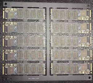
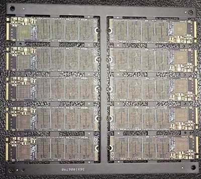
Bare Board PCB
Bare board PCBs represent the starting point for all electronic assemblies. Ready for the good part? These boards arrive without components, featuring only copper circuitry, substrate layers, solder mask, and silkscreen. You handle assembly, soldering, and testing in-house or at a contract manufacturer. The key components include conductive copper traces patterned according to your Gerber files, drilled holes for vias and through-holes, and protective coatings that guard against oxidation.
At its core, a bare board PCB consists of a dielectric substrate—often FR-4 or polyimide—for mechanical support and electrical insulation. Conductive pathways etched into copper foil connect pads and vias, defining the circuit topology. A solder mask layer covers non-conductive regions, preventing shorts during soldering, while silkscreen labels aid assembly alignment and inspection. This clear separation between bare board production and component assembly helps you optimize each stage for cost and quality.
Manufacturers produce bare boards in large volumes, leveraging photolithography, etching, drilling, and plating steps to meet tight tolerances. Quality checkpoints adhere to IPC-6012 standards, ensuring copper etch accuracy, hole quality, and board flatness. From single-layer prototypes through complex multilayer designs, bare boards serve industries from consumer electronics to aerospace. Their role remains pivotal: without a reliable bare board, component yields drop and field reliability suffers.
| Attribute | Description |
|---|---|
| Definition | Unpopulated PCB with copper traces and substrate |
| Substrate | Commonly FR-4, polyimide, ceramic |
| Conductive Layer | Copper foil etched into circuit patterns |
| Protective Coating | Solder mask for insulation and silkscreen for labeling |
| Role in Manufacturing | Foundation for component assembly and in-circuit testing |
Manufacturing a bare board PCB starts with precise patterning of copper on a substrate, ensuring your design transfers without error. But here’s the kicker… each step demands micron-level accuracy or you face short-circuits or open circuits at assembly. First, a dry-film photoresist coats the copper-clad substrate. Ultraviolet light exposes circuit patterns from your Gerber files onto this resist. Unexposed areas rinse away, revealing copper underneath. Next comes chemical etching, where an etchant solution removes unwanted copper, leaving only the desired traces and planes.
After etching, drilling creates holes for through-hole components and vias. Modern shops use CNC drills guided by drill files, achieving hole tolerances of ±0.05 mm. Laser drilling handles microvias in multilayer boards, enabling high-density interconnects without disturbing adjacent layers. What’s the real story? Proper drill maintenance and bit selection prevent burrs and misregistrations that could derail your yield.
Once holes are drilled, copper plating forms conductive barrels inside vias. Electroplating deposits copper uniformly, achieving thickness specified by you—often 10–25 µm inside each via. Then lamination stacks and bonds prepreg and core layers under heat and pressure for multilayer boards. This lamination ensures layer-to-layer adhesion and alignment within 0.1 mm. After lamination, final imaging, etching, and drilling refine internal and external layers.
Quality control intervenes at every stage. Automated optical inspection checks trace adhesion and resist definition after etching. X-ray inspection verifies via fill and alignment. Electrical testing uses flying probes or bed-of-nails fixtures to confirm continuity and isolation across thousands of nets. Only boards passing strict IPC-6012 criteria move on to solder mask and silkscreen application. This solder mask adds 20–40 µm of protection, while silkscreen applies component reference labels with 0.1 mm resolution.
By isolating bare board production from component assembly, you maintain specialized workflows that drive cost efficiency and quality. From simple single-sided prototypes to 20-layer rigid-flex solutions, this manufacturing sequence guarantees a reliable foundation for every B2B electronics program.
| Step | Process Detail | Tolerance/Standard |
|---|---|---|
| Photoresist Imaging | UV exposure of dry-film resist | ±0.05 mm pattern resolution |
| Copper Etching | Chemical removal of unwanted copper | ±0.1 mm trace width accuracy |
| Drilling | CNC and laser drilling for vias and holes | ±0.05 mm hole positional tolerance |
| Via Plating | Electroplating for conductive via walls | 10–25 µm copper barrel thickness |
| Lamination | Bonding of layers under heat and pressure | 0.1 mm layer-to-layer registration |
| Optical Inspection | Automated checks for trace integrity | IPC-6012 Class 2 acceptance |
| Electrical Testing | Continuity and isolation via flying probe or fixtures | 100% net verification |
Bare board PCBs rely on a precise combination of materials whose properties determine board performance under electrical load and environmental stresses. But here’s the kicker… selecting the right substrate and copper grade can make the difference between board failure in the field and long-term reliability on your production line. At the foundation stands the substrate. FR-4 remains the industry mainstay thanks to its favorable balance of mechanical strength, low cost, and electrical insulation. It consists of woven fiberglass cloth bonded with flame-retardant epoxy resin. This is where it gets interesting… alternative substrates like polyimide deliver superior thermal stability and flexibility, proving ideal for high-temperature or flex-circuit applications in automotive and aerospace programs.
Copper foil provides the conductive layer. Standard boards use 1 oz copper (35 µm) per square foot, but bare boards often employ 2 oz or 3 oz grades for higher current capacity. Heavy copper options (up to 10 oz) handle several dozen amps per trace with minimal voltage drop. Ready for the good part? Dielectric adhesives and prepregs bind multilayer stack-ups under heat and pressure, ensuring layer-to-layer adhesion and consistent dielectric thickness. These epoxy resin films impregnated with glass fiber control impedance and permit precise drilling of microvias.
Protective surface finishes guard copper from oxidation and improve solderability. HASL (hot air solder leveling) remains common because of low cost, but immersion silver and OSP (organic solderability preservative) appeal to lead-free assembly workflows, offering flat, solder-friendly surfaces without tin splatter. Silkscreen inks then apply component designators and logos, aiding assembly and inspection.
Each material choice carries trade-offs in cost, manufacturability, and performance. FR-4 substrate suits most control-logic boards, whereas polyimide or ceramic substrates shine in RF or high-power modules. What’s the real story? Your bare board vendor should provide datasheets detailing Tg (glass transition temperature), CTE (coefficient of thermal expansion), dielectric constant, and loss tangent so you can match material properties to your operating environment. By understanding these materials, procurement and engineering teams can partner with fabricators on boards that meet electrical, mechanical, and regulatory demands without unexpected rework or field returns.
| Material | Key Property | Typical Use Case |
|---|---|---|
| FR-4 Substrate | Tg ~130 °C, moderate CTE | General-purpose PCBs |
| Polyimide Substrate | Tg ~260 °C, low CTE | Flex circuits, high-temp electronics |
| Copper Foil (1–10 oz) | Conductivity 58 MS/m | Varying current-load requirements |
| Prepreg/Epoxy Resin | Dielectric bonding layer | Multilayer core lamination |
| HASL Finish | Lead-tin protective coating | Cost-sensitive assemblies |
| OSP Finish | Organic solderability preservative | Lead-free, flat surface needs |
| Immersion Silver | Fine pitch, flat finish | High-density SMT designs |
| Silkscreen Ink | Assembly reference labels | Date codes, part identifiers |
Bare board layout demands precision from start without sacrificing manufacturability. Ready for the good part? Begin by defining trace width and spacing that match copper weight and expected current loads. Narrow traces on heavy copper boards fail under stress if widths don’t scale. Measure trace width against copper thickness using IPC-2152 formulas or vendor guidelines so loss remains within acceptable limits. Layer stack-up planning follows. What’s the real story? A balanced stack-up prevents warpage and ensures impedance control for high-speed nets. Position reference planes evenly above and below signal layers, and maintain consistent dielectric thickness to stabilize impedance values.
Via strategy plays a central role. Microvias suit multilayer inner pairs and high-density interconnect boards, while traditional drill vias work for through-hole components and power planes. Tailor via pad sizes and annular ring dimensions to fabricator capabilities. Plan for thermal relief pads around large copper pours to simplify soldering. Otherwise you’ll see tombstoning or solder voids that disrupt yield.
Thermal management enters every design conversation for power assemblies. Add copper pours on outer layers and stitch them to inner planes with thermal vias that conduct heat away from hotspots. This is where it gets interesting… Stitch arrays of 20–50 vias under power components to guarantee uniform heat flow. Meanwhile guard against over-etching fine features; maintain minimum copper etch tolerances your fabricator certifies, often ±10 µm for 100 µm trace widths.
Clearance rules also govern solder mask slivers. Maintain 0.1 mm solder mask web widths between pads on fine-pitch components to avoid mask lifting. Silkscreen legend placement must avoid via annular rings and mask dams that could smear or bleed during screen printing. Always confirm that silkscreen inks meet UL 94 V-0 standards if boards serve safety-critical equipment.
Finally, check design data with a thorough DRC (design rule check) against IPC-2221 or IPC-6012 Class 2 requirements. This prevents mechanical failures, reduces rework, and cuts cycle time. By focusing on trace geometry, stack-up balance, via configuration, thermal relief, and mask integrity, you deliver bare boards that support reliable assembly and peak performance every run.
| Design Parameter | Recommendation | Impact on Production |
|---|---|---|
| Trace Width | ≥ 3 × copper weight in oz | Ensures current capacity and reduces heating |
| Trace Spacing | ≥ 2 × minimum line width | Prevents shorts and supports panel yield |
| Stack-Up Balance | Even layer dielectric thickness | Minimizes warpage and maintains impedance |
| Via Type | Microvias for dense layers, thru-holes for power | Improves routing and thermal conduction |
| Thermal Vias | Arrays under high-power parts | Enhances heat dissipation and reliability |
| Solder Mask Web Width | ≥ 0.1 mm between pads | Avoids mask peeling and assembly issues |
| Silkscreen Placement | Clear of pads and vias | Prevents ink smearing and misalignment |
| DRC Standard | IPC-2221 or IPC-6012 Class 2 | Ensures manufacturability and quality |
But here’s the kicker… inspecting bare board PCBs catches defects early when corrections cost minutes rather than days. Manufacturers implement layered inspection strategies that blend visual, automated, and electrical tests to confirm every trace, via, and mask feature meets spec. Visual checks start with trained operators under high-intensity lamps examining panel edges, drill holes, and copper traces for burrs or residue. Any stray whisker or over-etched line spotted here prevents assembly failures down the line. What’s the real story? Automated optical inspection (AOI) follows, using high-resolution cameras that scan each board against golden files. AOI flags issues like missing pads, thin traces, or solder mask misregistration. This machine vision step achieves repeatable detection rates above 99 percent, far beyond manual limits.
Next comes X-ray inspection for inner layers and hidden vias. X-ray systems reveal misdrilled holes, voided copper fills, and inner layer misalignment that AOI cannot see. Spotting a misregistered inner trace at this stage avoids scrap of fully laminated boards. Ready for the good part? Electrical testing uses flying probes or bed-of-nails fixtures. Flying probes offer flexible, low-cost net verification ideal for prototypes and small batches. They confirm continuity and isolation across thousands of nets by applying contact probes to pads guided by test files. Bed-of-nails fixtures suit high-volume production, enabling simultaneous contact to every test point and rapid in-circuit testing at hundreds of boards per hour.
Some vendors add environmental stress tests such as thermal cycling or humidity exposure on sample boards to validate resin adhesion and copper plating integrity under extreme conditions. Burn-in tests under power replicate real-world loads, uncovering latent faults before panels ship. Effective inspection marries speed, coverage, and accuracy. By layering visual, AOI, X-ray, and electrical tests, you gain confidence that every bare board meets IPC-6012 Class 2 requirements. This rigorous approach cuts down rework, ensures first-pass yield, and keeps your assembly lines humming without unexpected stoppages.
| Inspection Stage | Method | Purpose |
|---|---|---|
| Visual Inspection | Manual under bright lights | Detect surface defects and contamination |
| AOI | Automated optical cameras | Verify trace integrity and mask alignment |
| X-ray Inspection | X-ray imaging | Reveal inner layer misregistration and voids |
| Flying Probe Test | Programmable probe contact | Confirm continuity and isolation for prototypes |
| Bed-of-Nails Test | Fixed-pin fixture | Rapid net testing in high-volume production |
| Environmental Stress | Thermal cycling/humidity tests | Validate material and plating reliability |
But here’s the kicker… ensuring bare board quality starts by aligning your design and fabrication against established industry benchmarks that guarantee reliability and consistency across batches. The key standard is IPC-6012, which specifies qualification and performance requirements for rigid PCBs. It covers parameters such as copper thickness, plating integrity, hole tolerances, and dielectric strength. Manufacturers reference IPC-6012 Class 2 for general electronic products and Class 3 when demanding high reliability in aerospace or medical equipment. This is where it gets interesting… IPC-2221 sets generic design rules including minimum trace width and spacing, insulation resistance, and thermal performance. By validating your Gerber files against these rules you catch layout errors before boards reach production.
UL 94 provides flammability ratings for substrate materials used in bare boards. A board rated V-0, for example, must extinguish flame within 10 seconds, critical for safety-certified applications. Meanwhile RoHS and REACH regulations restrict hazardous substances such as lead, mercury, and certain flame retardants. Compliance requires material declarations and testing reports ensuring no banned substances exceed defined thresholds. Ready for the good part? IEC 61189 outlines test methods for mechanical, electrical, and environmental performance of PCB materials and finished bare boards, including humidity, thermal cycling, and dielectric breakdown tests.
Each standard plays a unique role: IPC governs design and acceptance criteria, UL assesses safety under fire conditions, RoHS/REACH enforces environmental compliance, and IEC defines test procedures. Top-tier fabricators maintain certification and audit reports, proving adherence to each. When selecting a vendor ask for IPC certificates and UL listings for your specific board type. Request material test reports showing RoHS and REACH compliance. What’s the real story? Boards built to these standards suffer fewer field failures, reduce warranty claims, and streamline global market entry.
| Standard | Scope | Key Requirements |
|---|---|---|
| IPC-6012 | PCB qualification and performance | Copper thickness, hole tolerances, dielectric tests |
| IPC-2221 | Generic design rules | Trace/spacing rules, thermal parameters |
| UL 94 | Flammability of materials | V-0 to V-2 ratings for substrate fire resistance |
| RoHS/REACH | Restriction of hazardous substances | Limits on lead, mercury, cadmium, PBDEs |
| IEC 61189 | Test methods for PCB materials | Humidity, thermal cycling, dielectric breakdown |
Multilayer bare boards stack several core and prepreg layers to achieve complex routing and high-density interconnects. Ready for the good part? Unlike single- or double-sided boards, multilayer constructions interleave signal and plane layers, enabling compact designs with controlled impedance and reduced noise. Each internal layer undergoes its own etching and inspection before lamination. This means tighter tolerances—often ±0.05 mm registration between layers—yet it yields boards with eight, twelve, or more copper layers capable of supporting hundreds of nets within a small footprint. Designers plan layer allocation strategically: power and ground planes serve as reference layers, sandwiched between signal layers to minimize loop inductance and EMI.
Building multilayers begins by imaging and etching each core. Prepreg sheets—epoxy resin impregnated fiberglass—bond cores under heat and pressure. But here’s the kicker… lamination pressures exceed 10 bar and temperatures reach 180 °C to ensure void-free adhesion. Post-laminate drilling then penetrates all layers, requiring precise drill bit control to avoid smear or delamination. Via options multiply: through-holes span all layers, blind vias connect outer to inner layers, and buried vias link internal pairs. This via diversity allows high-density routing without sacrificing board rigidity.
Thermal management becomes more critical. Heat generated in inner layers must traverse multiple substrates and copper planes. Designers incorporate thermal vias that connect heat sources on outer layers down to internal ground planes. Thermal simulations identify hotspots before fabrication. This is where it gets interesting… specialized prepreg materials with low dielectric loss tangent optimize high-frequency signal integrity in RF multilayer boards.
Testing also intensifies. Automated X-ray inspection checks internal layer alignment and via fill quality, while flying probe tests verify continuity across complex layer stacks. Only boards meeting IPC-6012 Class 3 for multilayer reliability advance to surface finishes.
Multilayer bare boards shine in telecommunications, server backplanes, and aerospace electronics where space, performance, and signal integrity matter most. Their construction demands rigorous process control and design foresight, but the payoff is printed circuit boards that pack more functionality into less real estate without compromising quality.
| Feature | Single/Double-Sided PCBs | Multilayer PCBs |
|---|---|---|
| Layer Count | 1–2 copper layers | 4–20+ copper layers |
| Routing Density | Limited outer-layer routing | High-density internal and external routing |
| Impedance Control | Basic trace geometry | Controlled dielectric spacing per layer |
| Via Types | Only through-holes | Through, blind, and buried vias |
| Lamination Pressure | Not required | ≥10 bar at 180 °C |
| Inspection Methods | AOI and electrical tests | X-ray, AOI, and advanced electrical tests |
Protective finishes guard copper surfaces from oxidation and ensure solderability during assembly. What’s the real story? HASL—hot air solder leveling—remains widespread thanks to its low cost and good solder wetting. Boards pass through molten solder, then hot air knives remove excess, leaving a uniform tin-lead or lead-free coating approximately 3–5 µm thick. Despite slight surface unevenness, HASL suits through-hole assemblies and wide-pitch SMT.
Immersion silver offers a flat, solder-friendly finish ideal for fine-pitch applications. Ready for the good part? Silver deposit thickness typically ranges from 0.1–0.4 µm, with low contact resistance and excellent surface planarity. However, silver migration under high humidity demands careful storage and handling.
OSP—organic solderability preservative—uses a thin organic film that bonds chemically to copper. With a coating thickness of 0.2–0.5 µm, OSP leaves boards flat and oxide-free. It excels in lead-free wave and reflow soldering but requires controlled rework practices since multiple solder cycles can erode the protective film.
Immersion tin provides a robust Sn finish of 1–3 µm. It resists oxidation and delivers flat surfaces for micro-BGA and QFN packages. Tin finishes can age over time, forming whiskers if improperly handled, so manufacturers often add whisker-mitigation steps.
ENIG—electroless nickel immersion gold—deposits a 3–6 µm nickel barrier with 0.05–0.1 µm gold on top. This is where it gets interesting… ENIG offers excellent shelf life, planar surface, and gold’s superior corrosion resistance, making it a premium choice for high-reliability and fine-pitch boards. The nickel layer prevents copper diffusion, while the gold ensures solder wetting during assembly.
Selecting the right finish balances cost, assembly process, and reliability. HASL suits general-purpose boards, while ENIG or immersion silver ranks higher for high-density or high-reliability target markets.
| Finish Type | Thickness | Key Benefits | Considerations |
|---|---|---|---|
| HASL | 3–5 µm | Low cost, good wetting | Uneven surface, not ideal for fine-pitch |
| Immersion Silver | 0.1–0.4 µm | Flat planarity, low resistance | Susceptible to migration |
| OSP | 0.2–0.5 µm | Flat surface, lead-free friendly | Limited reflow cycles |
| Immersion Tin | 1–3 µm | Good solderability, flat finish | Tin whisker risk |
| ENIG | Ni 3–6 µm, Au 0.05–0.1 µm | Excellent shelf life, fine-pitch | Higher cost |
Electrical verification prevents costly rework by validating nets before assembly. But here’s the kicker… bare boards contain thousands of nets, each requiring both continuity and isolation checks. Flying probe testing delivers flexibility: programmable probes contact pads based on test files derived from your PCB CAD’s netlist. Each probe pair applies voltage and measures current flow, confirming that copper traces connect intended nodes and remain isolated from adjacent nets. Flying probe testers cover up to 5,000 nets per board in under ten minutes, making them ideal for prototypes and low-volume runs.
In high-volume production, bed-of-nails fixtures dominate. Custom fixtures hold boards in place while spring-loaded pins simultaneously contact every test point. This is where it gets interesting… bed-of-nails tests can validate 100 percent of nets in seconds, ensuring rapid throughput. They perform continuity checks across copper planes, high-pot tests to verify insulation resistance under high voltage, and resistive-impedance measurements that catch thin-copper or etching anomalies.
Continuity tests apply a small voltage (<5 V) and expect a low resistance (<5 Ω) across connected nets. Isolation tests apply higher voltage (50–100 V) and expect no current flow between neighboring nets. High-pot tests ramp voltage up to product-specific thresholds (up to 1,000 V) for dielectric breakdown assessment. Ready for the good part? custom test programs include looping structures that validate complex multi-layer stack-ups and detect buried internal faults invisible to visual inspection.
Data logging captures every test result, generating yield metrics and failure analytics. Boards failing electrical tests divert automatically to rework stations. Engineers review failure logs to pinpoint design or process improvements—reducing yield loss and boosting production efficiency. Combined with AOI and X-ray before testing, electrical tests complete a robust quality framework ensuring bare boards meet your exact B2B specifications before assembly ever begins.
| Test Method | Voltage Range | Purpose | Throughput |
|---|---|---|---|
| Flying Probe | <5 V continuity, 50–100 V isolation | Flexible net-by-net testing for prototypes | 5–10 minutes/board |
| Bed-of-Nails Fixture | <5 V continuity, up to 1,000 V high-pot | Mass-production full-board testing | <30 seconds/board |
| Continuity Check | <5 V | Confirm intended connections | Included in both |
| Isolation Test | 50–100 V | Ensure no shorts between nets | Included in both |
| High-Pot Test | Up to 1,000 V | Validate dielectric strength | Production-critical |
But here’s the kicker… reliability for bare board PCBs hinges on rigorous validation at every process step so end products withstand real-world stresses. Manufacturers employ accelerated stress tests replicating temperature swings and humidity extremes that boards will face in the field. Thermal cycling subjects panels to repeated heating above 100 °C then cooling below 0 °C for dozens of cycles. Boards that crack or delaminate under these conditions never reach customer floors. This is where it gets interesting… humidity testing exposes boards to up to 85 percent relative humidity at 85 °C. Insulation resistance measurements before and after confirm no deterioration in dielectric barriers.
Mechanically, boards undergo solder float tests, where heated solder bath exposure for 90 seconds verifies mask adhesion and copper plating resilience. Bending tests flex boards 90° to simulate shock and vibration in transportation. Boards passing these endure forklift drops and assembly line impacts without broken traces. Ready for the good part? chemical resistance tests immerse samples in cleaning agents—alkaline or mildly acidic—ensuring solder mask and silkscreen remain intact after board washes.
Electrical reliability features long-term bias tests. A board repeatedly powered under rated voltages for 168 hours checks for leakage and dielectric breakdown. Constant current stress testing pushes copper traces to rated current loads for extended periods, revealing thermally induced failures like copper migration or pad lift.
Supplier quality programs require lot traceability, where each panel links back to material batches and machine logs. Statistical process control charts monitor drill bit wear, etch bath concentration, and plating bath purity, identifying drift before boards fail. Collecting failure data feeds continuous improvement, reducing defect opportunities by over 50 percent year over year.
Ultimately bare board reliability combines standardized stress tests, real-time process control, and feedback loops so you receive panels built for high first-pass yield and field durability across consumer, automotive, and industrial applications.
| Test Type | Condition | Pass Criteria |
|---|---|---|
| Thermal Cycling | 100 °C ↔ 0 °C, 50 cycles | No delamination or crack |
| Humidity Test | 85 °C, 85 % RH, 96 hours | Insulation resistance >10⁶ Ω |
| Solder Float | 260 °C, 90 seconds | No mask lift or copper blistering |
| Bend Test | 90° bend, 5 cycles | No trace cracks or conductor separation |
| Bias Burn-In | Rated voltage, 168 hours | Leakage current < specified threshold |
Bare boards serve diverse sectors from consumer gadgets to harsh-environment electronics. What’s the real story? consumer electronics makers rely on single- and double-sided boards for smartphones, wearables, and home automation devices. High volume and tight cost targets demand rapid bare board cycles and consistent yields. Automotive and EV applications push demands higher; battery management systems and power distribution modules use multilayer bare boards with controlled impedance and heavy copper layers for current handling up to 30 A per trace. Ready for the good part? automotive boards also require automotive-grade substrates rated to 150 °C and compliance with AEC-Q100 for component reliability.
Industrial machinery and robotics incorporate bare boards in motor drives and programmable controllers. These boards handle high voltages and currents, often built with 4 oz copper and ceramic substrates for heat spread. Medical device manufacturers adopt bare boards in diagnostic imaging and implantable electronics. These boards must meet ISO 13485 and UL 60601-1 standards for safety and biocompatibility.
Aerospace and defense sectors demand bare boards that survive radiation, extreme temperatures, and vibration. Exotic substrates like polyimide or teflon deliver low outgassing and high thermal stability. Boards for satellites and avionics undergo Level 3 reliability testing under MIL-PRF-31032 protocols. This is where it gets interesting… network infrastructure and telecom providers use high-speed backplane bare boards with HDI microvias supporting 56 Gb/s data rates in data centers.
Each industry pairs specific bare board requirements with assembly processes. From quick-turn prototypes for startups to fully certified production runs for mission-critical systems, bare boards remain the universal foundation driving electronics innovation across markets.
| Industry | Board Type | Key Requirements |
|---|---|---|
| Consumer Electronics | Single/double-sided PCBs | High volume, cost-effective |
| Automotive & EV | Multilayer, heavy copper | 30 A+ current, automotive-grade substrates |
| Industrial Machinery | 4 oz copper, ceramic substrates | High voltage, thermal management |
| Medical Devices | FR-4/polyimide, UL 60601-1 | Biocompatibility, safety certifications |
| Aerospace & Defense | Polyimide, teflon, MIL-PRF-31032 | Radiation tolerance, vibration resistance |
| Telecom/Networking | HDI microvias | 56 Gb/s+ signal integrity |
Understanding cost drivers helps you balance performance and budget. Here’s the deal… base substrate choice impacts price significantly. FR-4 runs $2–5 per sq in, whereas polyimide boards can cost 2–3× more. Copper weight drives material costs: 1 oz copper boards remain baseline, while 3 oz or 4 oz copper adds 20–50 percent to raw material expense. But here’s the kicker… each extra layer in a multilayer stack-up adds prepping, imaging, etching, drilling, plating, and lamination steps—easily $5–10 per layer on small batches.
Board complexity factors—fine-line traces below 4 mil, microvias, blind vias—require advanced equipment and controlled processes, adding $1–3 per sq in. Surface finishes also affect cost: HASL stays under $0.05 per sq in, immersion silver adds $0.10, and ENIG may reach $0.30. Tight tolerances for impedance control, such as ±5 percent, elevate inspection and process controls, tacking on 10–20 percent to overall PCB cost.
Volume discounts apply. Prototype runs under 10 panels often incur $100 setup fees plus $50 per panel. In quantities above 100, per-panel pricing can drop 50–70 percent. Ready for the good part? consolidating panel sizes and optimizing nesting efficiency reduces waste and lowers per-board cost by up to 15 percent.
Turnaround times influence pricing. Standard 10–15 day deliveries follow published rates; expedited services add 25–50 percent premiums for 3–5 day cycles. International shipping and customs further impact landed cost for global procurement teams.
By mapping bare board specifications—copper weight, layer count, surface finish, complexity—against budget constraints, you achieve cost-performance balance. Early collaboration with fabricators on DFM reviews uncovers cost-saving adjustments without sacrificing board integrity.
| Cost Factor | Price Impact | Typical Range |
|---|---|---|
| Substrate Choice | 1–3× baseline | FR-4: $2–5/sq in |
| Copper Weight | +20–50 % per extra oz | 1 oz to 4 oz copper |
| Layer Count | +$5–10 per additional layer | Single to 20-layer |
| Advanced Features | +$1–3/sq in (microvias, fine lines) | Depends on density |
| Surface Finish | +$0.05–0.30/sq in | HASL to ENIG |
| Turnaround Time | +25–50 % for expedited | Standard vs 3–5 day run |
Selecting the right bare board vendor often determines project success or hidden delays. But here’s the kicker… not all fabricators handle every board type with equal skill. Start by verifying core certifications. Look for ISO 9001 quality management and IPC-A-600 or IPC-6012 compliance statements. These prove the shop follows industry guidelines for copper etch quality, material traceability, and mechanical tolerances. Next, evaluate copper weight capabilities. If your design calls for 3 oz or heavier copper, confirm the vendor’s plating lines support that thickness without warpage. Ask for sample boards reflecting your layer count and finish specifications, then inspect them for dimensional accuracy and finish consistency.
Technical support ranks just as high. This is where it gets interesting… the best manufacturers offer pre-production DFM reviews. They catch potential layout issues such as insufficient mask dams around fine-pitch pads or inadequate thermal via distribution. By looping in their engineers early, you reduce rework cycles and speed time to assembly. Capacity and lead time also matter. Small prototype runs need quick-turn services, often within 3–5 days, while volume production runs require the ability to handle panels by the hundreds or thousands without scheduling bottlenecks. Make sure their minimum order quantities align with your production ramp, avoiding excessive inventory or repeat setups.
Cost structure cannot be ignored. Seek transparent quotes that break out substrate, copper weight, layer count, and finish costs separately. Beware of bundled prices that obscure hidden fees for tracking number registration or expedited shipping. Try negotiating volume rates if you plan quarterly orders. Ready for the good part? Visit the vendor’s facility if possible. On-site tours reveal cleanliness, equipment age, and process controls that translate directly into board consistency. Check drill room practices for bit change frequency and etch bath maintenance schedules.
Finally, review past performance through client testimonials or case studies. A shop that handles automotive-grade bare boards under AEC-Q100 or medical PCBs under ISO 13485 has proven its mettle. By combining certification checks, technical collaboration, capacity assessments, clear costing, and real-world references, you secure a bare board partner that delivers quality panels on time and within budget.
| Selection Criterion | What to Verify | Why It Matters |
|---|---|---|
| Quality Certifications | ISO 9001, IPC-A-600, IPC-6012 | Ensures adherence to industry standards |
| Copper Weight Capability | Support for 1–10 oz copper plating | Determines current capacity and thermal handling |
| DFM Review Support | Pre-production design checks | Reduces rework and speeds assembly |
| Lead Time & Capacity | Prototype turnaround, volume order scheduling | Avoids production bottlenecks |
| Cost Transparency | Itemized quotes for substrate, layers, finishes | Prevents hidden fees |
| Facility Audit | On-site visit, equipment condition | Validates process controls |
| Client References | Case studies for automotive, medical, industrial boards | Confirms proven reliability |
Emerging technologies are rapidly shaping how bare boards meet next-generation requirements. This is where it gets interesting… High-density interconnect (HDI) techniques will spread further, placing microvias and laser-drilled blind vias at sub-100 µm pitches. This evolution allows consumer electronics and telecom backplanes to pack more traces into smaller footprints without sacrificing integrity. Meanwhile additive manufacturing shows promise. Experimental PCB printing methods build copper and dielectric layers with inkjet or aerosol jet systems, potentially reducing waste and setup time for complex multilayer boards. Look for pilot runs where these printed layers match or exceed traditional etch performance under stress.
Automated optical inspection lines are also gaining AI-powered vision tools that flag anomalies beyond simple pattern mismatches. These systems learn from failure data, catching over-etch or mask defects earlier and with higher accuracy. But here’s the kicker… sustainability drives adoption of greener substrates. Bio-based resin and recyclable fiberglass are entering pilot certifications, aiming to reduce hazardous waste at end of life. RoHS and REACH will extend to new material categories, tightening controls on brominated flame retardants and perfluorinated compounds.
Electrical performance demands continue rising. As GHz-level signal integrity becomes commonplace in 5G and beyond, bare boards must exhibit consistent dielectric constants across wide temperature ranges. New prepreg formulas with low loss tangents will become standard. Thermal management likewise advances; embedded heat pipes or metal core materials beyond aluminum—such as copper-invar-copper laminates—might appear in high-power modules. Ready for the good part? Integration of sensors within bare boards could enable real-time process monitoring. Imagine boards that report humidity ingress or thermal cycling counts before failure, allowing predictive maintenance.
Finally, global supply chains will see distributed bare board production hubs. Regional fabricators close to major electronics clusters reduce shipping times and carbon footprints. Coupled with digital twin verification—where your CAD model links directly to the shop floor—this trend makes prototyping or reruns nearly instant worldwide. By staying aware of HDI expansion, additive methods, advanced inspection, green materials, and embedded intelligence, electronics teams remain prepared for the bare board revolution in coming years.
| Trend | Description | Impact |
|---|---|---|
| HDI & Microvias | Sub-100 µm blind/microvias | Enables higher routing density |
| Additive PCB Printing | Inkjet or aerosol-jet copper and dielectric deposition | Reduces waste, speeds prototyping |
| AI-Powered AOI | Machine learning vision for defect detection | Higher accuracy, earlier catch rates |
| Green Substrates | Bio-resins, recyclable fiberglass | Lower environmental impact |
| Embedded Thermal Materials | Copper-invar-copper or integrated heat pipes | Improved heat spread in high-power modules |
| In-Situ Sensor Integration | Humidity and thermal cycle monitoring | Predictive maintenance |
Despite meticulous processes, bare board defects still occur. Ready for the good part? Warpage tops the list—it emerges when layer stack-ups remain unbalanced or lamination pressures vary. Even a 0.1 mm imbalance in dielectric thickness can twist boards beyond assembly tolerances. Mitigation calls for symmetrical layer distribution and strict lamination monitoring. Over-etching presents another headache. Excess etchant concentration or prolonged exposure attacks trace edges, turning designed 100 µm lines into 80 µm fragile webs. Implement real-time etch bath chemistry tracking and timed resist removal to avoid this.
Drill misregistration and burr formation can short rings around vias. Old or misaligned drill bits wander off pattern. But here’s the kicker… monthly drill bit calibration routines and wear logs slash misregistration by over 70 percent. Burrs clear via barrels and cause pad collapse under pressure. Automated brush and vacuum cleaning stations after drilling prevent metal shards from embedding in resin.
Solder mask scum and fish eyes appear when mask application parameters stray. Controlling mask viscosity and maintaining stencil cleanliness ensures even mask coverage. Silkscreen bleeding or missing prints often trace back to poor ink mixing or stencil wear. Replacing screens every 10,000 panels and batch-testing ink adhesion keeps legends crisp.
Finally copper plating voids in vias can hide internal connectivity breaks. These voids escape visual inspection but fail during electrical testing. This is where it gets interesting… adding mid-process X-ray checks at 50 kV accelerates void detection before final plating. Combined with plating bath purity monitoring, you maintain barrel fill rates above 99 percent.
By recognizing warpage, over-etch, drill defects, mask issues, and plating voids as the usual suspects—and applying balanced stack-ups, precise etch control, drill calibration, mask process discipline, and X-ray spot checks—you protect bare board yields and safeguard assembly success.
| Issue | Root Cause | Mitigation Strategy |
|---|---|---|
| Warpage | Asymmetric stack-up, lamination drift | Symmetrical layers, strict press controls |
| Over-Etch | Excessive etchant concentration/time | Real-time bath chemistry tracking |
| Drill Misregistration | Bit wear, alignment drift | Regular calibration, wear logs |
| Burr Formation | Inadequate chip evacuation post-drill | Automated brush/vacuum cleaning |
| Mask Scum | Viscosity and stencil issues | Viscosity checks, stencil maintenance |
| Silkscreen Bleed | Ink mixing, worn screens | Ink QC, screen replacement |
| Plating Voids | Bath impurities, plating line issues | Mid-process X-ray checks, bath purity tests |
Choosing a bare board PCB will address your assembly efficiency concerns by providing a robust foundation tailored to your design. You’ve seen how precise manufacturing steps, material choices, and stringent inspections build quality into every panel. Performance hinges on design rules, surface finishes, and reliability tests that match industry benchmarks. Now apply these insights—partner with a certified fabricator who offers design reviews, transparent costing, and advanced inspection. By focusing on proven processes and future-ready trends, you secure bare boards that minimize rework and maximize uptime. Reach out today for a DFM consultation and take the ambiguity out of PCB procurement.
FAQ
Q1: What is a bare board PCB?
A bare board PCB is an unpopulated printed circuit board with etched copper traces on a substrate, ready for component assembly.
Q2: How does photolithography work in PCB manufacture?
Photolithography applies UV light through a mask to pattern photoresist on copper foil, then developer removes unexposed resist before etching away unwanted copper.
Q3: What standards apply to bare board quality?
Key standards include IPC-6012 for performance and IPC-2221 for design, alongside UL 94 flammability and RoHS/REACH environmental compliance.
Q4: How is electrical testing performed on bare boards?
Testing uses flying probe or bed-of-nails fixtures to check continuity, isolation, and high-pot dielectric strength across all nets.
Q5: What causes PCB warpage and how is it prevented?
Warpage stems from unbalanced layer stacks and lamination issues; prevention uses symmetrical stack-ups and strict lamination pressure control.


Connect to a Jerico Multilayer PCB engineer to support your project!
Request A Quote


 Quote
Quote