


+86 13603063656
Multilayer PCB board: comprehensive guide, construction & uses. In today’s electronics-driven world, the multilayer PCB board has become the beating heart of innovation, enabling everything from smartphones to satellites. But here’s the kicker… many buyers and engineers still wonder: what exactly makes a multilayer PCB different from its single or double-sided cousins? Why are these boards the foundation of high-speed, compact, and powerful devices? This article is your step-by-step manual to the multilayer PCB board, covering its evolution, construction, materials, applications, design, and future trends. By the end, you’ll understand how multilayer PCB boards drive modern technology, why B2B buyers favor them, and what to look for when sourcing the right supplier. Ready for the good part? Let’s dive into every angle that matters for manufacturers, OEMs, engineers, and electronics business leaders.
Multilayer PCB Boards
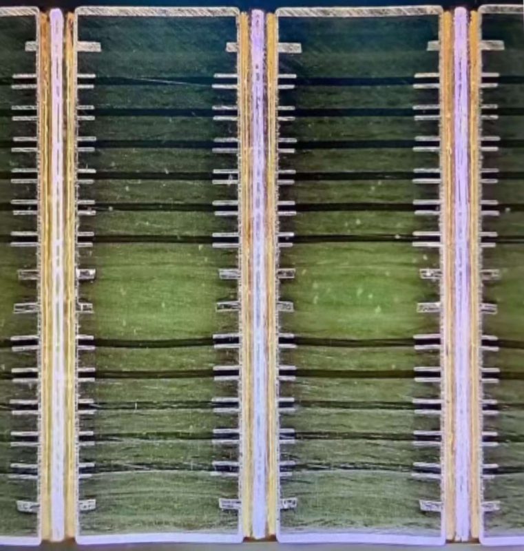
What’s the real story? The structure of a multilayer PCB board isn’t just stacking copper and insulation together—it’s about sophisticated engineering that allows complex circuitry in minimal space. Each board contains alternating layers of conductive copper and insulating substrate, usually built from an FR-4 or polyimide core. Think of it as a sandwich: the copper forms the bread, while the dielectric layers are the fillings, delivering electrical isolation between circuit layers. A typical multilayer PCB starts with a core (a double-sided board), to which layers of “prepreg” (pre-impregnated resin) and copper foil are laminated. The result? Boards with anywhere from four to 50+ layers, each carefully pressed and bonded to ensure electrical connectivity through plated through-holes, blind vias, or microvias. Each layer must align perfectly—registration errors can mean signal loss or short circuits. Copper thickness, layer arrangement, and insulating material type are all engineered to meet signal, thermal, and mechanical demands. This is where it gets interesting… modern multilayer boards can include embedded passive or active components within inner layers, further shrinking the size of electronic assemblies and boosting functionality.
Table: Typical Multilayer PCB Layer Stack-Up
| Layer Type | Material | Function |
|---|---|---|
| Outer Layer | Copper/Prepreg | Signal routing, solder pads |
| Prepreg (insulation) | Fiberglass/Epoxy | Electrical insulation |
| Core | Copper/FR-4 | Structural backbone, routing |
| Inner Signal Layer | Copper | Power, ground, or signal traces |
| Solder Mask | Epoxy Ink | Protects copper, aids assembly |
| Silkscreen | Epoxy Ink | Component labeling, markings |
But here’s the kicker… the real magic of multilayer PCB boards isn’t just in their construction, but in their power to transform electronics. First, multilayer PCBs deliver incredibly high circuit density. Need a tiny wearable with dozens of sensors, or a telecom switch with hundreds of interconnects? Multilayer boards can handle it, thanks to their multiple stacked layers that allow complex routing without crossing traces. Second, these boards excel in electrical performance. Why? Because designers can sandwich signal layers between ground and power planes, minimizing EMI and improving signal integrity at high speeds. Ready for the good part? Multilayer PCBs also improve power distribution by using dedicated layers for power and ground, reducing voltage drops and supporting robust, noise-free operation. Imagine a server motherboard or automotive ECU—these platforms depend on multilayer PCBs for reliable performance under tough conditions. The implication is clear: whether you’re in aerospace, IoT, or consumer devices, multilayer PCBs unlock features that single or double-sided PCBs simply can’t deliver.
Table: Key Advantages of Multilayer PCB Boards
| Advantage | Description |
|---|---|
| High Circuit Density | Supports compact, complex layouts |
| Enhanced Signal Integrity | Reduces crosstalk, EMI, and signal losses |
| Improved Power Delivery | Dedicated planes for stable voltage supply |
| Smaller Form Factor | Enables device miniaturization |
| Increased Reliability | Stronger structure, fewer interconnections needed |
This is where it gets interesting… multilayer PCB boards are everywhere, and their applications are expanding every year. In consumer electronics, think smartphones, tablets, and laptops—each packed with high-speed processors and wireless modules, all riding on intricate multilayer PCBs. Automotive engineers rely on these boards for engine control units, infotainment systems, and advanced driver-assistance systems (ADAS), where reliability and size are critical. In telecom, multilayer boards enable network switches, base stations, and routers to deliver gigabit speeds and dense interconnects. Ready for the good part? The medical sector uses multilayer PCBs in diagnostic equipment, imaging systems, and implantable devices, where precision and miniaturization are life-saving. Industrial automation and aerospace applications round out the picture, requiring boards that withstand harsh environments, vibration, and thermal cycling.
Table: Leading Applications of Multilayer PCBs
| Industry | Example Applications |
|---|---|
| Consumer | Smartphones, tablets, laptops |
| Automotive | Engine control, ADAS, infotainment |
| Telecom | Routers, switches, network hardware |
| Medical | MRI, CT scanners, implants |
| Industrial | Robotics, PLCs, industrial controls |
| Aerospace | Avionics, satellites, navigation |
But here’s the kicker… every material in a multilayer PCB board is selected for a reason. Start with the core: FR-4 is the most common, prized for its balance of cost, mechanical strength, and electrical insulation. Polyimide substrates come into play when you need thermal stability—think aerospace or automotive. Copper, the hero of conductivity, is used in various thicknesses (typically 0.5 oz to 3 oz per ft²) depending on current load. Prepreg—glass fiber woven and saturated with epoxy resin—serves as the glue between layers, offering insulation and dimensional stability. What’s the real story? Surface finishes also matter. Options like HASL, ENIG, or OSP protect copper from oxidation and support reliable soldering during assembly. Each choice impacts thermal performance, cost, and lifespan, making material selection a crucial step in design and procurement.
Table: Key Materials in Multilayer PCBs
| Material | Typical Use | Key Benefits |
|---|---|---|
| FR-4 | Core/Prepreg | Good strength, electrical insulator |
| Polyimide | High-temp applications | Flexible, excellent heat resistance |
| Copper Foil | Signal & power layers | High conductivity |
| Prepreg | Layer bonding | Stable, good adhesion |
| ENIG/HASL/OSP | Surface finish | Solderability, oxidation resistance |
Ready for the good part? Designing a multilayer PCB board is as much about art as engineering. Start with layer stack-up: how many layers are needed? The answer depends on signal complexity, EMI shielding, and required board thickness. Signal routing is another challenge—high-speed signals must be kept short and shielded by adjacent ground planes to avoid noise. Differential pairs, impedance control, and return path planning all play a role. Don’t forget thermal management! High-current traces, power-hungry components, and tight layouts generate heat—careful layer placement, thermal vias, and copper pours help dissipate it. What’s the real story? Collaboration between electrical and mechanical design teams is vital to avoid conflicts between circuit needs and housing constraints.
Table: Key Multilayer PCB Design Considerations
| Design Aspect | Impact on Performance |
|---|---|
| Stack-Up Planning | Controls EMI, supports signal speed |
| Impedance Control | Maintains signal integrity |
| Thermal Design | Prevents overheating |
| Via Management | Enables dense routing |
| Mechanical Layout | Ensures fit within device enclosure |
But here’s the kicker… manufacturing a multilayer PCB board is a high-precision dance. It starts with prepping the inner cores—cleaning, imaging with photoresist, and etching traces. Next comes stacking: alternating layers of core, prepreg, and copper foil are pressed together under heat and pressure to create a solid laminate. Drilling follows—holes for vias and through-holes are formed, often by laser for microvias or CNC for standard vias. Once drilled, the holes are plated with copper to ensure electrical connection across layers. Imaging and etching are repeated for outer layers. Solder mask is applied, followed by silkscreen for labeling. Then, the boards are routed to shape and surface finished. Inspection, AOI, electrical testing, and final QC round out the process, catching any defects before shipment. This sequence ensures each multilayer PCB meets tight tolerances for high-reliability industries.
Table: Steps in Multilayer PCB Manufacturing
| Process Step | Description |
|---|---|
| Core Imaging | Patterning inner layers |
| Lamination | Pressing stack-up under heat/pressure |
| Drilling | Creating vias and through-holes |
| Plating | Depositing copper in holes and traces |
| Etching | Defining outer layer circuitry |
| Solder Mask | Insulating/protecting copper |
| Silkscreen | Printing labels and reference marks |
| Testing | AOI, electrical, and mechanical checks |
What’s the real story? Vias are the unsung heroes of multilayer PCB boards—they connect different layers, allowing signals and power to travel up and down the stack. The simplest is the through-hole via, which passes from top to bottom. Blind vias connect an outer layer to one or more inner layers, while buried vias connect only internal layers. Microvias—tiny laser-drilled holes—are essential for HDI (High-Density Interconnect) boards, supporting dense, high-speed layouts. Ready for the good part? Choosing the right via type reduces board size, increases routing density, and enables advanced features like stacked or staggered via structures in 5G and IoT applications.
Table: Types of Vias and Their Features
| Via Type | Description | Best Use Case |
|---|---|---|
| Through-Hole | Connects all layers | Power, large component pins |
| Blind | Connects outer to inner layers | HDI, dense BGA footprints |
| Buried | Internal layers only | Complex, compact layouts |
| Microvia | Laser-drilled, very small | HDI, fine-pitch, mobile |
Ready for the good part? Every multilayer PCB board undergoes rigorous inspection—because even a tiny flaw can cause major headaches downstream. Automated Optical Inspection (AOI) scans the board for shorts, opens, or misaligned features. Electrical testing (bed-of-nails, flying probe) checks that all nets are connected as intended and isolated where needed. What’s the real story? Mechanical testing might include thermal cycling, flex/bend tests, and solderability checks to ensure boards survive the stresses of real-world use. Only boards that pass these checks are shipped to the customer, giving you confidence that your investment meets IPC-6012 and industry-specific standards.
Table: Common Multilayer PCB Tests
| Test Type | Purpose | Equipment Used |
|---|---|---|
| AOI | Visual inspection of traces/features | High-res cameras, AOI system |
| Flying Probe | Electrical continuity/isolation | Robotic test system |
| Bed-of-Nails | High-volume electrical testing | Fixture with spring probes |
| Thermal Cycling | Reliability under temp changes | Environmental chamber |
| Solderability | Assembly process check | Solder bath, wetting tests |
But here’s the kicker… the cost of a multilayer PCB board can vary dramatically based on several factors. The more layers you add, the higher the cost—not just for material, but for every process step from lamination to drilling and testing. Complex via structures (blind, buried, or microvias) push up costs due to advanced equipment and process controls. Material choice matters too: polyimide and heavy copper add to the bill. Ready for the good part? Large production runs offer economies of scale, while fast-turn or prototype orders command premiums. Suppliers may also charge extra for special surface finishes or tight tolerances, so it’s crucial to specify exactly what you need up front.
Table: Key Cost Factors in Multilayer PCB Production
| Factor | Impact on Cost | Notes |
|---|---|---|
| Layer Count | Increases cost | More layers = more steps |
| Via Type | Adds complexity/cost | HDI, microvia = higher cost |
| Material Selection | Premium for specialty | Polyimide, heavy copper |
| Production Volume | Reduces per-unit cost | Larger orders = discounts |
| Turnaround Time | Expedited = more costly | Prototype vs. standard lead |
But here’s the kicker… even the best multilayer PCB design can hit roadblocks. Delamination—where layers separate—can occur if lamination isn’t done perfectly or if moisture is trapped. Warping is another issue: thin, asymmetrical boards or improper cooling during processing can cause bowing, making boards hard to assemble. What’s the real story? Crosstalk and EMI are headaches in dense, high-speed layouts, but are managed by careful stack-up and ground plane placement. Quality assurance, from material inspection to final test, is the key to minimizing these risks. Ready for the good part? Partnering with an experienced manufacturer with robust process controls and a track record of troubleshooting complex boards helps you avoid costly surprises.
Table: Multilayer PCB Challenges & Solutions
| Challenge | Root Cause | Solution/Best Practice |
|---|---|---|
| Delamination | Moisture, lamination error | Proper storage, process control |
| Warping | Asymmetry, cooling issues | Balanced stack, controlled temp |
| EMI/Crosstalk | Poor layout, stack-up design | Layer planning, ground planes |
| Registration | Misalignment during lamination | Automated alignment systems |
| Solderability | Contaminants, finish issues | Cleanliness, quality finish |
This is where it gets interesting… the multilayer PCB board industry is innovating fast. Embedded components—resistors, capacitors, even chips—can now be placed within inner layers, shrinking size and enhancing performance. Flexible and rigid-flex multilayer PCBs support foldable devices and aerospace components, offering both high density and mechanical flexibility. Additive manufacturing techniques, like 3D printing with conductive inks, are emerging for rapid prototyping. Advanced materials—halogen-free, low-loss, or ultra-thin dielectrics—enable next-gen telecom and wearable devices. These innovations open new horizons for what’s possible in design, cost, and reliability.
Table: Innovations in Multilayer PCB Technology
| Innovation | Description | Key Benefit |
|---|---|---|
| Embedded Components | Passive/active parts inside layers | Smaller, faster, more reliable |
| Rigid-Flex Boards | Combination of rigid and flexible | Dynamic, space-saving designs |
| Additive Processes | 3D printed circuitry | Fast prototyping, new materials |
| Low-Loss Materials | Advanced substrates for RF/microwave | Better high-speed performance |
| Halogen-Free PCBs | Environmentally friendly | Meets green standards |
But here’s the kicker… not all multilayer PCB suppliers are created equal. Start with capabilities: does the manufacturer support the layer counts, via structures, and finishes you need? Certification matters too—look for ISO 9001, UL, IPC-6012, and any sector-specific credentials. What’s the real story? Evaluate their design-for-manufacturing (DFM) support—can they help optimize your files before production? Always request samples and review quality data from previous runs. Ready for the good part? Communication is key; you want a partner who responds quickly, provides clear quotes, and solves problems proactively. Site visits, audits, and referrals from trusted clients also help ensure you’re working with a reliable, experienced supplier who can deliver on time, every time.
Table: Manufacturer Evaluation Checklist
| Evaluation Factor | What to Look For | Why It Matters |
|---|---|---|
| Technical Capability | Layers, HDI, finishes | Supports your design needs |
| Certifications | ISO, UL, IPC, sector-specific | Ensures process quality |
| DFM/Support | Early-stage engineering input | Reduces rework, saves money |
| Quality Data | Yield, defect rates, test logs | Demonstrates reliability |
| Communication | Responsive, clear, proactive | Prevents costly delays |
Ready for the good part? The multilayer PCB board industry isn’t slowing down—it’s shifting gears for the future. Miniaturization continues as wearable tech, IoT, and 5G demand denser, thinner boards. Green manufacturing—using eco-friendly materials and cleaner processes—is becoming a must for global brands. AI-driven design and simulation tools will make board layout smarter, faster, and more reliable. Smart PCBs, with embedded sensors and self-monitoring capabilities, are on the horizon. What’s the real story? The suppliers who invest in R&D and adapt to these trends will be the ones who lead tomorrow’s electronics revolution.
Table: Future Trends in Multilayer PCBs
| Trend | Description | Potential Impact |
|---|---|---|
| Miniaturization | Smaller, denser, thinner boards | Drives wearables/IoT |
| Green Materials | Halogen-free, recyclable options | Sustainability, compliance |
| AI-Driven Design | Automation, simulation | Faster, better designs |
| Smart PCBs | Embedded monitoring/sensors | Predictive maintenance |
| 5G/High-Frequency | Ultra-high speed, low-loss boards | Telecom, data center growth |
Multilayer PCB board: comprehensive guide, construction & uses—now you’ve seen it all. The multilayer PCB board is the unsung hero of modern electronics, powering everything from the latest wearables to mission-critical aerospace equipment. Its complex structure, material choices, design rules, and manufacturing precision create a platform for reliability
and innovation. But here’s the kicker… working with a certified, capable supplier is just as important as the design itself. By staying informed on the latest trends and best practices, you can specify and source multilayer PCB boards that support your business goals and keep your products ahead of the curve. Ready for the good part? Your next project could set the standard for the entire industry—choose your multilayer PCB partner wisely.
Q1: What is a multilayer PCB board?
A multilayer PCB board is a printed circuit board with three or more layers of conductive copper, laminated together with insulating material, supporting dense and complex electronic circuits.
Q2: How does the multilayer PCB manufacturing process work?
It involves imaging, stacking, laminating, drilling, plating, etching, applying solder mask and silkscreen, then rigorous electrical and visual testing before delivery.
Q3: What advantages do multilayer PCBs offer over single-sided boards?
They provide higher circuit density, improved signal integrity, smaller device size, better power management, and enhanced reliability for advanced applications.
Q4: What materials are typically used in multilayer PCBs?
Common materials include FR-4 (fiberglass/epoxy), polyimide, various grades of copper foil, prepreg, and different surface finishes like ENIG or HASL.
Q5: How can I choose the right multilayer PCB manufacturer?
Look for suppliers with experience, technical capability, industry certifications, DFM support, strong quality records, and clear, proactive communication.


Connect to a Jerico Multilayer PCB engineer to support your project!
Request A Quote


 Quote
Quote