


+86 13603063656
Large PCB boards play a pivotal role in today’s high-power and high-complexity electronic environments. But here’s the kicker… many designers and buyers aren’t even sure what actually qualifies as a “large” PCB board! While there’s no global standard, the term generally refers to any printed circuit board exceeding typical panel sizes, often starting at dimensions above 300mm x 400mm. These boards are used where real estate is at a premium—think industrial power supplies, large LED arrays, high-end servers, and telecommunications infrastructure.
Let’s dig a bit deeper. Standard PCB sizes often top out at around 244mm x 305mm, but large-format boards can measure up to 600mm or even more in length or width. What’s the real story? Large PCB boards are engineered to accommodate more components, higher current flows, and complex routing requirements that simply can’t fit on a standard board.
You’ll find these boards wherever power and signal must travel over significant distances, or where heavy components demand extra surface area for thermal management. The implications? Larger boards often face new challenges in warpage, handling, and design complexity. Yet the benefit is clear: more space for creativity and integration.
| Size Category | Typical Dimensions | Common Applications |
|---|---|---|
| Standard | ≤ 244mm x 305mm | Consumer electronics, IoT |
| Mid-size | 245–300mm x 305mm | Networking, Industrial |
| Large | ≥ 300mm x 400mm | Power, LED, Telecom, Data |
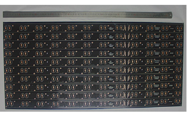
Large PCB Board
Ready for the good part? The adoption of large PCB boards in industry is driven by necessity—not just by desire. Industrial applications push the limits of current, voltage, and complexity, demanding more expansive circuit real estate than smaller boards can offer.
Think about these scenarios: Power distribution cabinets in energy plants rely on large PCBs to route thick copper traces for massive current. Industrial automation systems, like those in robotics or manufacturing lines, need large-format boards to handle dense I/O and robust connectors. In telecommunications, base stations require expansive boards for high-frequency signal paths and power management.
But here’s the real story: Large PCB boards make it possible to combine power, signal, and control on a single, unified platform. That’s a huge leap for design efficiency and reliability. Consider LED street lighting panels—each large board might handle hundreds of LEDs, complete with drivers, heat sinks, and monitoring circuits. Or picture railway control systems: large PCBs support the redundancy, reliability, and ruggedness required for such safety-critical environments.
Here’s another point—industrial settings demand easy maintenance and modularity. Large PCB boards allow designers to group related functions on one board, making repair and upgrade much easier. The net result? Reduced downtime and simplified inventory.
| Industry Sector | Large PCB Application | Benefit |
|---|---|---|
| Power Distribution | High current, relay boards | Reliability, safety |
| Industrial Automation | Dense I/O, connectors | Flexibility, scalability |
| Telecom | RF, backplane, power | High data rates, density |
| Rail/Transport | Safety, control | Robustness, maintainable |
But what’s the real story behind the types of large PCB boards? There’s more variety here than you might think. Let’s break it down: Large PCB boards can be single-sided, double-sided, or multilayer. Single-sided boards are rare at this size, as most applications require double-sided or multilayer designs to maximize routing efficiency.
Here’s where it gets interesting… Rigid, flexible, and rigid-flex PCBs can all be produced in large formats. For instance, large rigid PCBs dominate power and industrial spaces, but some medical imaging equipment or aerospace assemblies use oversized flex or rigid-flex boards for lightweight, space-constrained builds.
Layer count is another key differentiator. Large PCB boards may range from simple two-layer designs to complex 12-layer or even higher stacks, especially in telecommunications or high-performance computing. Each format presents unique manufacturing, handling, and reliability challenges.
Material choices abound too. Standard FR-4 remains the workhorse, but you’ll see high-Tg, polyimide, and even aluminum-based boards in large sizes. The goal? Match material characteristics to performance, durability, and cost.
| Board Type | Typical Layer Count | Best For | Notes |
|---|---|---|---|
| Rigid | 2–20+ | Industrial, power, telecom | Stiff, robust |
| Flex | 1–8 | Aerospace, medical | Lightweight, bendable |
| Rigid-Flex | 4–16 | Medical, defense | Complex, expensive |
Designing a large PCB board isn’t just scaling up a standard layout. Here’s the kicker: New challenges emerge as the physical size increases. Trace routing, signal timing, and layer stack-up all demand more detailed planning and analysis. PCB design software must handle larger coordinate grids, longer traces, and more complex netlists.
But what’s the real story? Managing crosstalk, impedance, and propagation delay is exponentially harder when traces stretch for hundreds of millimeters. Designers often break up the board into logical zones for power, analog, digital, and RF sections. This zoning minimizes noise and EMI.
Let’s get practical—component placement takes on a new dimension. Heavy components need reinforcement or extra mounting points. Long traces can act as unwanted antennas if not carefully managed. Engineers must also account for board flexure during handling or operation, adding mechanical support where needed.
Finally, don’t overlook file formats: Design outputs like Gerber, ODB++, and IPC-2581 need to capture extensive detail for manufacturing. Review cycles are longer, and close communication with fabricators is critical to avoid costly errors.
| Design Aspect | Key Consideration | Impact on Large PCBs |
|---|---|---|
| Trace Routing | Length, impedance, noise | Timing, signal integrity |
| Zoning | Power/analog/digital/RF split | Noise, EMI management |
| Stack-Up | Layer count, material choice | Performance, yield |
| File Format | Gerber, ODB++, IPC-2581 | Clarity, manufacturability |
Ready for the good part? Large PCBs introduce challenges that don’t exist in standard formats. Warpage and mechanical deformation are primary concerns—long boards can bend or twist during manufacturing, assembly, or even shipping.
But here’s the kicker… Signal integrity and EMI issues are amplified at scale. Long traces become transmission lines, susceptible to delay and interference. Designers must add extra ground planes, controlled impedance traces, and shielding to ensure performance.
Thermal management gets tough too. Large boards often dissipate more power, so thermal vias, copper pours, and dedicated heat sinks are common. Think about power distribution—a single trace may need to handle 50A or more, requiring careful width calculation and copper thickness.
There’s another hidden challenge: Handling and assembly. Oversized boards may require custom fixtures, special conveyors, or manual processes. Even soldering can be more difficult due to temperature gradients across the board.
In short, large PCB board design is not for the faint of heart—but with the right expertise, these obstacles become manageable.
| Challenge | Description | Mitigation |
|---|---|---|
| Warpage | Mechanical distortion | Ribs, thicker material |
| Signal Integrity | Crosstalk, noise, delay | Zoning, shielding, layout |
| Thermal Management | Hot spots, power density | Heat sinks, vias, copper |
| Handling/Assembly | Manual, custom fixtures | Training, automation |
What’s the real story? Material choice can make or break a large PCB project. While FR-4 is the industry workhorse, its limitations show up quickly in oversized boards with high thermal or mechanical demands.
But here’s the kicker… High-Tg FR-4, polyimide, metal-core (aluminum or copper), and advanced laminates are all contenders for large boards. High-Tg materials resist warping and maintain strength at elevated temperatures. Metal-core substrates help spread and dissipate heat, crucial for power and LED applications.
Copper thickness also comes into play. Standard 1oz copper might suffice for signals, but power traces often require 2oz, 3oz, or even 6oz layers. Surface finishes—HASL, ENIG, OSP—must be chosen for compatibility with both assembly process and reliability targets.
Material cost and lead time escalate with size and specialization, so early consultation with suppliers saves headaches later.
| Material Type | Best Use Case | Strength | Limitation |
|---|---|---|---|
| FR-4 | General, low–mid power | Cheap, available | Warpage, thermal limits |
| High-Tg FR-4 | Mid–high power, size | Strength, heat resistant | More costly |
| Metal-core | Power, LEDs | Heat dissipation | Heavy, not flexible |
| Polyimide | Aerospace, flex | Lightweight, durable | Expensive |
What’s the real story? Manufacturing large PCB boards requires specialized equipment, larger panel sizes, and skilled technicians. Here’s the kicker… Every process step—drilling, etching, plating, solder mask, and testing—faces new scale-related challenges.
Drilling must account for long tool paths and increased flex. Plating tanks and conveyor ovens must accommodate greater board length. Even screen printing of solder mask and legend becomes more complex, requiring tight tension control and registration.
Panelization, depanelization, and handling steps are also key—oversized boards are heavier, harder to move, and more prone to bending. Some shops use vacuum lifting or robotic transfer to prevent damage. Inspection for large PCBs may require AOI (automated optical inspection) setups with expanded fields of view.
Don’t forget about yield: The risk of defects grows with size, so process capability and quality control are critical.
| Manufacturing Step | Large PCB Challenge | Solution/Note |
|---|---|---|
| Drilling | Long holes, flex | Rigid fixtures, slow speed |
| Plating | Uniformity, coverage | Special tanks, agitation |
| Screen Printing | Tension, registration | Robust screens, automation |
| AOI/Testing | Size, coverage | Multi-head, custom setup |
But here’s the kicker… Quality control for large PCB boards is an order of magnitude more demanding than for standard boards. Inspection stations must be physically larger and more advanced to spot defects across expansive surfaces.
Automated optical inspection (AOI) machines are reconfigured for extra-wide panels. X-ray inspection can reveal hidden solder joint or via problems, especially in multilayer boards with BGAs or heavy copper.
Electrical testing is a must—flying probe or bed-of-nails setups are scaled up for size. But the real story? Every defect costs more, both in material and process time, so prevention is far better than rework.
Traceability matters, too. Barcode labeling and process logs track each board through the workflow, tying every lot to detailed process records. This data is invaluable for root-cause analysis if field failures ever occur.
| QC Method | Purpose | Benefit |
|---|---|---|
| AOI | Surface defect detection | Fast, high coverage |
| X-ray | Internal structure check | Finds hidden issues |
| Electrical Test | Continuity, shorts | Ensures circuit function |
| Traceability | Process tracking | Root-cause, quality proof |
Ready for the good part? Assembly of large PCB boards pushes the limits of standard SMT and through-hole processes. Long boards might not fit in conventional reflow ovens or pick-and-place machines, necessitating custom lines or manual operations.
Component placement must account for thermal gradients—parts at one end of a long board may heat or cool faster than others during reflow, risking solder defects. Here’s the real story: Heavy components can stress solder joints, so extra anchors or epoxy underfill may be required.
Manual assembly and inspection are often needed, especially for unique or oversized connectors. Rework and repair are also more complex; large boards can’t be moved easily and may require in-place troubleshooting.
Packaging and ESD protection take on new urgency—the stakes are simply higher when dealing with expensive, hard-to-replace boards.
| Assembly Method | Large PCB Challenge | Solution/Note |
|---|---|---|
| SMT | Machine size limits | Custom lines, manual work |
| Reflow | Thermal gradients | Profiling, zoned ovens |
| Through-Hole | Long, heavy parts | Reinforcement, hand-solder |
| Inspection | Access, ESD risk | Special tables, covers |
What’s the real story? Shipping and storage of large PCB boards is a logistical exercise in risk management. Boards are more vulnerable to mechanical and ESD damage during handling, packing, and transit.
But here’s the kicker… Oversized anti-static bags, custom foam inserts, and heavy-duty cartons are standard for transport. For high-value shipments, crating and vibration damping may be used. Some manufacturers even use climate-controlled storage to minimize moisture uptake and warpage risk.
Barcoding and lot tracking ensure traceability throughout warehousing and logistics chains. Safe handling training for staff is a must. Failure to protect these boards at this stage can render thousands of dollars’ worth of product useless.
| Protection Method | Use Case | Advantage |
|---|---|---|
| ESD Bags | All shipments | Static protection |
| Foam Inserts | Heavy, fragile boards | Shock absorption |
| Crating | Oversized, export | Structural integrity |
| Barcoding | All warehousing | Traceability |
Ready for the good part? Failure modes for large PCB boards go beyond what’s typically seen in smaller formats. Warpage during assembly can create open or short circuits. Solder joint failures are more common, especially at board edges or heavy component locations.
Let’s not forget delamination, where heat and mechanical stress split board layers, leading to reliability nightmares. Heavy copper and dense traces can exacerbate this risk if process control slips. Another troublemaker: Via or pad lift-off, caused by mechanical shock during handling or installation.
EMI and crosstalk are heightened on large boards, potentially causing functional errors or intermittent faults. Each of these issues has a direct impact on product performance, yield, and warranty costs.
| Failure Mode | Cause | Impact |
|---|---|---|
| Warpage | Heat, handling | Open/short circuits |
| Solder Joint Fail | Thermal, mechanical stress | Intermittent, hard fault |
| Delamination | Poor lamination, heat | Layer separation, failure |
| Pad/Via Lift | Mechanical shock | Loss of connection |
But here’s the kicker… Not every PCB shop is equipped to handle large boards! Selecting the right manufacturer means looking for proven experience, up-to-date machinery, and strong process controls.
Ask about maximum supported board size, layer count, and copper thickness. Inquire about thermal profiling, assembly line compatibility, and AOI/X-ray inspection capability. Don’t just take their word—request samples, certifications (ISO, UL), and customer references.
Technical support is critical: You want a supplier who can review your design files, offer feedback, and propose improvements for yield and reliability. Look for clear communication, transparent pricing, and the ability to handle both prototyping and volume runs.
| Manufacturer Factor | Why It Matters | What to Check |
|---|---|---|
| Max Board Size | Fit for your needs | Machine spec sheets |
| QC/Inspection | Quality, reliability | AOI, X-ray, test systems |
| Technical Support | Design, troubleshooting | Engineer availability |
| Certifications | Industry standard | ISO, UL, customer audits |
Ready for the good part? Costing for large PCB boards includes more than just materials and labor. Material waste, setup, yield loss, and special handling all play a significant role.
Material cost jumps with board size, especially with thicker copper, high-Tg, or metal-core substrates. Manufacturing and assembly costs increase due to lower panelization efficiency, higher rejection risk, and longer processing times. Don’t overlook logistics—shipping oversized items is pricier.
Price breaks may be available at higher volumes, but prototyping or low-quantity runs are always more expensive per piece. The real story: Early collaboration with suppliers on design for manufacturability can help minimize cost surprises and boost yield.
| Cost Driver | Impact on Price | Notes |
|---|---|---|
| Material | High for size, specialty | Copper, substrate, finish |
| Processing | Longer, riskier | More handling, defects |
| Assembly | Manual, complex | Larger machines/labor |
| Logistics | Bulky, heavy | Special packaging/shipping |
What’s the real story? Large PCB board technology is advancing rapidly, driven by new material science, manufacturing automation, and smarter design tools.
Emerging trends include high-thermal-conductivity substrates, embedded passive components, and laser-drilled microvias. Automation is making panel handling, inspection, and testing more reliable and scalable. Digital twin and simulation tools help engineers predict board behavior before physical prototypes are built.
In green energy and automotive fields, large boards with integrated sensors and power management ICs are becoming standard. Plus, supply chain improvements and global logistics are reducing lead times and opening up new manufacturing geographies.
| Innovation Trend | Industry Impact | Example |
|---|---|---|
| High-Thermal Substrate | Power, LEDs | Al-based, ceramics |
| Embedded Passives | Size, performance | Filtered, decoupled lines |
| Laser Drilled Microvia | Density, signal integrity | Telecom, high-speed comp. |
| Automation | Cost, quality, repeatability | AOI, robotic handling |
on Large PCB Boards?**
Let’s bring it all together. Large PCB boards open new possibilities for industrial, power, telecom, and high-reliability applications. But here’s the kicker… Their design, manufacturing, assembly, and logistics require a much higher level of planning, expertise, and investment.
Work closely with experienced suppliers, leverage modern materials and tools, and always design for quality and manufacturability. With careful attention to every phase—design, production, inspection, and shipping—your large PCB projects will deliver superior performance and value for your business.
Q1: What is a large PCB board?
A large PCB board is any printed circuit board with dimensions significantly exceeding industry norms, often used for power, industrial, and high-complexity applications.
Q2: How are large PCB boards manufactured?
They require specialized machinery, longer process steps for drilling, plating, and assembly, and more advanced inspection and quality control to handle the increased complexity and risk of defects.
Q3: What industries most commonly use large PCB boards?
Power distribution, telecommunications, industrial automation, renewable energy, and transportation all heavily rely on large PCB boards.
Q4: What materials are used in large PCB boards?
Options include standard FR-4, high-Tg laminates, polyimide, and metal-core substrates—each selected based on size, heat, and mechanical demands.
Q5: What are common problems with large PCB boards?
Issues like warpage, solder joint failure, delamination, and higher logistics risks are more common due to increased board size and complexity.


Connect to a Jerico Multilayer PCB engineer to support your project!
Request A Quote


 Quote
Quote