


+86 13603063656
Printed circuit boards (PCBs) are at the heart of every electronic system. While designers spend a great deal of time on layer counts, signal integrity, and copper thickness, a critical but sometimes overlooked mechanical issue is PCB Bow — the tendency of a board to warp or bend out of plane. In its simplest form, PCB Bow represents a permanent deformation that occurs when internal stresses, asymmetric layer construction, thermal cycles, or improper material handling cause the board to lose flatness.
This handbook begins by offering a clear definition of PCB Bow, its measurement and diagnosis, and the key prevention strategies available to manufacturers and designers. The goal is to integrate engineering rigor with practical, shop-floor experience.
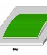
PCB Bow
PCB Bow arises from multiple sources. Some of the most common include:
Material Mismatch: Different coefficients of thermal expansion between copper and dielectric layers create internal stresses.
Asymmetric Stack-Ups: Uneven copper distribution or layer counts cause bending when released from lamination pressure.
High-Temperature Processing: Reflow soldering or wave soldering can induce residual stress, particularly if cooling is uneven.
Improper Storage or Handling: Boards stored vertically without support can slowly deform over time.
Understanding these root causes forms the foundation for any mitigation or prevention strategy.
Accurately quantifying PCB Bow is critical. Industry standards such as IPC-TM-650 and IPC-A-600 describe bow and twist measurement procedures. Common methods include:
Dial Indicator Measurement: Placing the PCB on a flat surface and measuring deflection at multiple points.
Optical or Laser Scanning: High-precision 3D measurement to create a warpage map.
Automated Board Handling Systems: Inline measurement during manufacturing for continuous monitoring.
By applying consistent measurement techniques, manufacturers can compare data over time and evaluate process changes with confidence.
Warped boards cause multiple downstream issues:
Assembly Misalignment: SMT pick-and-place machines may misregister components on bent surfaces.
Solder Joint Integrity: Non-flat boards cause uneven solder paste thickness and poor reflow.
Mechanical Stress on Components: Rigid connectors, BGAs, and large IC packages are especially sensitive to board flatness.
The cumulative effect is reduced yield, higher rework rates, and potential long-term reliability problems in the field.
The drawbacks of PCB Bow are not merely cosmetic. They translate into quantifiable cost and risk:
Reflow Shadowing: Certain areas receive less solder or heat due to warpage.
Automated Test Inaccuracy: Flying probe or bed-of-nails testers assume a planar surface.
Customer Returns and Warranty Claims: End-users expect robust products, and a warped board undermines perception of quality.
Recognizing these drawbacks early allows both design and manufacturing teams to collaborate on prevention.
To address PCB Bow, manufacturers deploy a mix of design controls, process adjustments, and material choices:
Symmetrical Stack-Ups: Balancing copper distribution and dielectric thickness to minimize stress.
Controlled Cooling: Implementing fixtures or chill plates during reflow to ensure even temperature gradients.
Pre-Bake and Conditioning: Reducing moisture and stabilizing materials prior to high-temperature processes.
Mechanical Flattening: In some cases, specialized presses can flatten boards after lamination.
An excellent example of robust mitigation comes from JM PCB, which uses advanced lamination controls and stack-up simulation to reduce warpage before boards leave the factory.
Designers have a pivotal role in minimizing PCB Bow:
Avoid large copper pours on one side without balancing them on the opposite side.
Keep dielectric thicknesses consistent across layers.
Specify flatness tolerances on fabrication drawings to ensure suppliers know the acceptable limits.
Incorporate panelization strategies that reduce stress concentration near board edges.
Choosing the right laminate and copper type can dramatically influence warpage. High-Tg materials, low-CTE dielectrics, and reinforced cores offer better dimensional stability.
Accurate measurement of PCB Bow underpins every successful diagnostic program. Without objective data, it’s impossible to know whether a process change or material substitution has improved or worsened flatness. Several established techniques are commonly used:
Dial Indicator / Height Gauge on Granite Surface:
The board is supported at its corners on a certified flat granite block, and a dial indicator measures deflection at specified points. This low-tech but effective method remains popular for spot checks and prototype evaluation.
Automated Optical Inspection (AOI) with Warpage Maps:
High-end AOI systems can measure three-dimensional profiles in seconds. They output a full color “heat map” showing warpage amplitude and direction.
Laser Scanning or White-Light Interferometry:
For mission-critical boards (aerospace, defense), laser scanning captures micron-level deviations from flatness.
IPC Standards:
IPC-TM-650 provides test methods for bow and twist. IPC-A-600 defines acceptability criteria. By adhering to these, manufacturers maintain consistency across global supply chains.
Consistently applying one of these methods and documenting results lets engineers track how changes in stack-up, lamination cycle, or storage conditions influence PCB Bow.
Assembly lines depend on precision. A PCB that is out of plane, even by fractions of a millimeter, can trigger a cascade of process disruptions:
Stencil Printing Defects: Uneven surfaces lead to variable solder paste thickness and bridging.
Pick-and-Place Errors: Modern placement heads assume a flat plane. Bowed boards can shift fiducials or alter component Z-heights, increasing misplacement risk.
Solder Joint Voiding or Opens: BGAs and fine-pitch components are particularly sensitive; even a slight warp can leave hidden open joints.
Long-Term Reliability: Stress on solder joints or connectors during product use can accelerate fatigue, especially in high-vibration environments.
By correlating assembly yield data with warpage measurements, engineers can determine how much PCB Bow is truly acceptable for their products.
Beyond yield loss, PCB Bow produces several knock-on effects:
Inspection Complexity: Automated test equipment (ATE) must adapt to uneven boards, adding cost.
Rework Difficulty: Attempting to reflow or flatten assembled boards can damage components.
Aesthetic Perception: Even if functionally acceptable, a visibly warped board signals poor quality to customers.
Logistics Problems: Bowed boards may not fit standard trays or automated conveyors, slowing throughput.
Recognizing these drawbacks early leads to proactive design and process adjustments rather than costly firefighting after production starts.
Manufacturers deploy a blend of preventive and corrective measures:
Balanced Stack-Ups: Maintain symmetry across the neutral axis. For every thick copper area, add balancing copper or dummy traces on the opposite layer.
Tight Lamination Controls: Precisely control press cycle, pressure, and temperature ramp.
Material Conditioning: Pre-baking laminates at specified temperatures drives off moisture and reduces residual stress.
Flattening Fixtures: Some facilities use post-lamination flattening presses to reduce bow before routing.
Controlled Cooling and Storage: Cool boards uniformly, store horizontally with full support.
As one industry example, JM PCB integrates simulation software that predicts warpage at the quotation stage. This allows designers to adjust their stack-up before fabrication, lowering risk.
Designers wield enormous influence on PCB Bow outcomes. Some actionable guidelines include:
Copper Balancing: Place dummy copper areas or hatched patterns opposite large pours.
Even Dielectric Thickness: Avoid major variations that could create a bending moment.
Panelization Strategy: Use tabs or rails that provide symmetrical mechanical support during reflow.
Specify Flatness on Drawings: Do not assume the supplier knows acceptable limits — state maximum bow/twist in millimeters per length.
These design moves cost little but yield major dividends in assembly yield and mechanical reliability.
Materials matter. High-Tg epoxy, low-CTE polyimide, and reinforced substrates all improve dimensional stability. Copper foil choice also influences warpage behavior.
Assembly engineers can also mitigate bow:
Use Dedicated Reflow Carriers or Pallets: Support the entire board perimeter and key internal zones.
Optimize Thermal Profiles: Gentle ramps and uniform heating reduce differential expansion.
Strategic Component Placement: Avoid clustering heavy components on one area of the board.
By treating assembly as part of the flatness solution, manufacturers close the loop between fabrication and end product.
The earliest opportunity to minimize PCB Bow is during schematic capture and layout planning. Decisions made at this stage are “baked in” and are far harder to correct later.
Key guidelines include:
Symmetry Above All: Keep the stack-up symmetrical across the board’s neutral axis. This means matching copper thicknesses, dielectric thicknesses, and glass styles.
Balance Large Copper Areas: Where a ground plane occupies one layer, mirror it on the opposite side with similar copper weight or use hatched copper if signal routing prohibits full copper fill.
Consider Component Weight Distribution: Place heavier or heat-generating components in a balanced pattern to avoid mechanical distortion during assembly.
Use Standard Board Thicknesses: Suppliers have proven process windows for common thicknesses. Exotic thicknesses increase lamination complexity and may lead to bow.
Specify Acceptable Bow/Twist Limits on Fabrication Drawings: IPC guidelines offer limits such as 0.75% for surface mount boards. Explicitly stating these numbers in the drawing enforces accountability.
Although we covered basic material concepts in Part 2, preventive control goes deeper:
Glass Transition Temperature (Tg): Higher Tg means the material remains stable at elevated reflow temperatures.
Coefficient of Thermal Expansion (CTE): A lower CTE closer to copper’s expansion reduces internal stress.
Filler Systems and Glass Weaves: Newer laminate systems use special filler particles and balanced glass weaves to minimize warp.
Copper Foil Type and Treatment: Selecting rolled copper foil in critical layers can improve mechanical properties.
Example: Automotive electronics often adopt low-CTE, high-modulus substrates because boards must survive temperature swings from -40 °C to +125 °C without excessive warp.
Panelization decisions strongly influence PCB Bow. Preventive practices include:
Symmetrical Panel Borders (Rails): Ensure equal support on all edges during reflow.
V-Scoring vs. Routing: V-scoring retains more edge material and can reduce warp, but it’s less flexible for odd-shaped boards.
Breakaway Tabs with Mouse-Bites: Use them judiciously to support critical areas.
Panel Orientation: Align the longest board dimension with the conveyor direction to minimize sag.
Preventive measures at assembly time include:
Rigid Carriers or Pallets: Particularly important for thin or large-format boards.
Thermal Profiling: Use even heating, minimal temperature differentials, and longer soak times to relieve stress gradually.
Component Placement Strategy: Distribute high-mass components evenly.
Reflow Under Vacuum: Some advanced lines use vacuum reflow to minimize voiding and warpage simultaneously.
Treat warpage as a process variable and chart it over time. For instance, record bow/twist at three points per board on every production lot, then create X-bar and R charts. Trend lines reveal drift early and enable corrective action before boards exceed specification.
People matter. Even the best processes fail if technicians handle boards incorrectly or ignore flatness metrics. Prevention culture includes:
Operator Training: Teach correct storage, handling, and inspection.
Visual Aids: Post clear flatness criteria at workstations.
Feedback Loops: Encourage operators to report unusual board behavior before it escalates.
Because materials and processes vary across suppliers, strong collaboration reduces risk:
Joint Stack-Up Reviews: Designer, fabricator, and assembler meet early to align on copper balance and material selection.
Flatness Tolerances in Contracts: Ensure purchase orders specify acceptable bow/twist percentages.
Supplier Audits: Evaluate how suppliers measure and control bow/twist.
Thermal management features such as metal cores, heat sinks, or thick copper planes influence board flatness:
Metal Cores: Provide rigidity but introduce CTE mismatch with FR-4.
Embedded Heat Spreaders: Must be symmetrically placed to avoid bending moments.
Thermal Vias: Improve heat dissipation but can alter local stiffness if concentrated in one area.
Designers must model thermal and mechanical behaviors together to avoid unintended PCB Bow.
Modern simulation tools allow engineers to predict warpage before a single board is built. FEA integrates material properties, stack-up, copper distribution, and thermal cycles to forecast bow and twist.
Benefits:
Reduce prototypes.
Quantify the effect of design changes quickly.
Optimize panelization strategies.
By making simulation routine, companies achieve faster design cycles and fewer production surprises.
Integrating PCB Bow mitigation techniques into recognized industry standards is a forward-thinking strategy for manufacturers who want to ensure high quality. Standards like IPC-A-600, IPC-6012, and IPC-2221 include guidelines for allowable bow and twist in printed circuit boards. However, manufacturers can go beyond compliance by developing internal quality metrics. By incorporating strict tolerances, measuring actual bow during production, and mandating preventive processes (such as symmetrical copper distribution and controlled lamination pressure), the organization signals its commitment to long-term reliability.
Another dimension is auditing and supplier qualification. Contract manufacturers and material suppliers should demonstrate how they control PCB Bow risks. Audits may include checks of equipment calibration, lamination press maintenance, and storage conditions of raw materials. By standardizing supplier quality and internal processes, the risk of unpredictable board deformation is minimized across the supply chain.
While PCB Bow is most often discussed in the context of rigid PCBs, its influence extends into high-density interconnect (HDI) and even rigid-flex or pure flexible circuits. In HDI designs, microvias, stacked vias, and thin dielectric layers make the board more susceptible to mechanical stress. Bow can cause registration errors between layers, leading to poor yields or latent reliability issues.
In flexible circuits, bow manifests differently — typically as unwanted curling or lack of flatness that complicates component placement or bonding to rigid sections. This is especially challenging in hybrid assemblies where rigid and flexible sections coexist. Addressing PCB Bow at the design stage for these advanced technologies involves careful material selection, layer balancing, and simulation of bending stresses to ensure that the final assembly remains within acceptable tolerances.
Modern CAD tools and finite element simulation platforms allow designers to model PCB Bow before fabrication. By simulating heat cycles, mechanical loads, and material responses, engineers can predict where and how bow might occur. This predictive approach is much more cost-effective than reactive correction during production.
CAD-driven design rules can automatically flag unbalanced copper areas, excessive cutouts, or irregular layer stacks. Some tools can even generate a “bow risk map” to guide adjustments in real time. When simulation results are combined with empirical shop-floor data, manufacturers can create a closed-loop feedback system that improves designs over time and minimizes bow-related scrap.
Automated assembly lines depend on precise component placement. Even a small PCB Bow can cause pick-and-place machines to misalign components, leading to open circuits or solder bridges. This is particularly critical for fine-pitch components such as BGAs, QFNs, and chip-scale packages.
To maintain placement accuracy, manufacturers deploy board support systems like vacuum plates, custom tooling pins, or conformal nests that ensure the board sits flat during placement. In addition, inspection systems such as 3D solder paste inspection (SPI) and automated optical inspection (AOI) can detect bow-induced defects early. By integrating preventive and corrective measures, the yield loss associated with bow at the assembly stage can be significantly reduced.
PCB Bow is not just a manufacturing inconvenience — it’s a reliability risk that can reverberate through design, assembly, and field performance. A holistic approach integrates:
Design Optimization: Balanced copper, symmetrical layers, and proper cutout placement.
Material Selection: Low-CTE cores, matched prepregs, and stable finishes.
Process Control: Calibrated equipment, predictive monitoring, and statistical feedback.
Strategic Partnerships: Leveraging expertise from suppliers like JM PCB to reduce risks and improve quality.
By viewing bow control as a continuous improvement cycle rather than a one-time fix, organizations can consistently deliver high-performance PCBs with fewer defects, higher yields, and greater customer satisfaction.
Controlling PCB Bow is not a one-dimensional task but an integrated discipline that spans design, material science, manufacturing engineering, and quality assurance. Throughout this handbook we have seen how imbalance in copper, asymmetrical stackups, thermal cycles, and uncontrolled processes can all generate warpage that jeopardizes yield, assembly accuracy, and long-term product reliability. Yet the same factors that create risk also create opportunity.
From my perspective, the most powerful shift is moving from reactive correction to proactive prevention. Design teams using simulation tools, balanced stackups, and predictive analytics can eliminate the majority of bow before the first panel is pressed. Manufacturers that rigorously calibrate their lamination presses, measure bow at multiple production stages, and work closely with trusted suppliers transform quality control from a cost center into a differentiator.
Another insight is that no single measure is sufficient. Material selection, process discipline, and equipment maintenance all reinforce one another. Partnerships with experienced fabricators like JM PCB, who understand how to optimize layer structures and pressing conditions, further reduce risk. Together, these actions form a closed-loop system in which every iteration of design and production feeds back to improve the next.
In the coming decade, the convergence of advanced materials, AI-driven process control, and more demanding end-use environments will only increase the importance of bow control. Those who master PCB Bow will not only reduce scrap and rework but also unlock higher reliability, lower total cost of ownership, and faster time to market.
Ultimately, PCB Bow need not be a chronic obstacle. With disciplined engineering, vigilant quality systems, and strategic supplier relationships, it becomes a manageable parameter — one that can be predicted, measured, and controlled. Organizations that embrace this approach will enjoy a sustained competitive edge in the ever-evolving electronics market.
FAQ 1: What is the difference between rolled copper foil and electrolytic copper foil?
Rolled copper foil is produced by mechanically rolling copper into thin sheets, offering better surface quality and mechanical strength. Electrolytic copper foil is deposited via an electrolytic process and is more flexible and cost-effective.
FAQ 2: How does copper thickness affect PCB Bow?
Thicker copper adds stiffness but also increases differential stress if unevenly distributed. If designers use heavier copper on one side without balancing it on the opposite side, bow and twist become more pronounced after lamination or reflow.
FAQ 3: Does using high-Tg material eliminate PCB Bow?
High-Tg laminates reduce the risk but do not eliminate it. Designers still need symmetrical stack-ups and proper copper balancing.
FAQ 4: How can storage conditions influence PCB Bow?
Storing boards vertically without support can lead to gradual warping under their own weight. Temperature and humidity cycling also induce stress. Always store horizontally with full support, in controlled humidity environments.
FAQ 5: Is it better to panelize or depanelize early to reduce PCB Bow?
Generally, keeping boards panelized until after major high-temperature processes helps distribute stress and prevents local distortion. However, the optimal approach depends on board size, component layout, and assembly line constraints.


Connect to a Jerico Multilayer PCB engineer to support your project!
Request A Quote


 Quote
Quote