


+86 13603063656

A PCB stencil is a vital tool used in the assembly of printed circuit boards (PCBs), specifically for applying solder paste onto the PCB surface. Proper use of a PCB stencil ensures that the soldering process is efficient and precise, directly affecting the overall quality and performance of the final product. In this article, we will explore the different types of PCB stencils, how they are used, and best practices for designing and maintaining stencils to achieve optimal results.
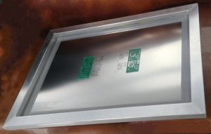
PCB Stencil
A PCB stencil is a thin sheet, often made of stainless steel or nickel, used in the solder paste printing process during PCB assembly. The stencil aligns with the PCB’s pad locations, and solder paste is spread through the stencil apertures to the corresponding pads on the PCB. The solder paste is then heated, causing it to melt and form solid solder joints for components placed on the PCB.
But here’s the kicker: PCB stencils are not just tools for applying solder paste—they are essential for achieving the accuracy and consistency needed in high-quality PCB manufacturing. Stencils help ensure that the right amount of paste is applied to the right locations, which is crucial for creating reliable solder joints that ensure the functionality of the final product.
Typically, PCB stencils are laser-cut to ensure precise aperture sizes and alignment with the PCB’s design. The stencil’s design plays a significant role in ensuring the solder paste is evenly applied, preventing common issues like insufficient solder or paste bridging between pads.
| Component | Description | Function |
|---|---|---|
| Stencil Material | Stainless steel, nickel, or other durable metals | Provides structure and durability for repeated use |
| Aperture | Holes cut in the stencil | Allows for the controlled application of solder paste |
| Alignment Pins | Pins to position the stencil | Ensures accurate placement on the PCB |
There are several types of PCB stencils, each designed for specific applications based on the complexity of the PCB and the required precision. Understanding the differences between these types is crucial for selecting the right stencil for your project.
What’s the real story? Each type of PCB stencil has unique features and advantages, and the right choice can dramatically impact your assembly process’s efficiency, quality, and cost.
| Stencil Type | Key Features | Common Applications |
|---|---|---|
| Laser-Cut Stencils | High precision, suitable for fine-pitch components | Ideal for most PCB assembly applications |
| Electroformed Stencils | Highly durable, excellent for small apertures | Best for high-volume production and fine-pitch designs |
| Nano-Coated Stencils | Coated to reduce paste adhesion | Used for high-speed production and fine-pitch components |
The manufacturing process of PCB stencils involves several steps, each requiring careful attention to ensure the stencil’s accuracy and quality. The choice of manufacturing method depends on the specific requirements of the PCB, such as the type of components, the size of the pads, and the complexity of the design.
Ready for the good part? The manufacturing of PCB stencils involves the precise cutting of apertures and the application of coatings to enhance their performance. This process ensures that the stencil is suited for high-precision paste application and can be reused multiple times in the production cycle.
| Step | Description | Purpose |
|---|---|---|
| Laser Cutting | Using a laser to cut stencil material | Achieves precise aperture sizes for high-density designs |
| Electroforming | Electroplating a metal onto a mold | Produces durable, high-precision stencils for fine-pitch designs |
| Nano-Coating | Applying a nano-coating to the stencil surface | Reduces solder paste adhesion, enhancing paste release |
PCB stencils are primarily used to apply solder paste to the surface of a PCB. However, their role extends beyond just paste application. Proper use of a PCB stencil helps ensure that the entire assembly process is efficient, reliable, and of high quality.
This is where it gets interesting: By using a PCB stencil, manufacturers can avoid common issues like insufficient paste application or paste bridging between pads, which can result in faulty solder joints. PCB stencils ensure that the right amount of paste is applied to each pad, allowing components to be soldered effectively and reliably.
| Function | Description | Impact on Production |
|---|---|---|
| Solder Paste Application | Applies solder paste to PCB pads | Ensures accurate and consistent paste application |
| Precision and Consistency | Ensures the same paste volume on every PCB | Reduces variation and defects in solder joints |
| Improved Assembly Speed | Speeds up the paste application process | Increases production efficiency and reduces cycle time |
The use of PCB stencils provides several key benefits in the PCB assembly process. These benefits directly impact the speed, cost, and quality of the manufacturing process, making stencils an indispensable tool for modern PCB assembly.
What’s the real story? By incorporating PCB stencils into the assembly process, manufacturers can improve production efficiency, reduce errors, and achieve better quality results. The benefits of using stencils are evident in the ability to mass-produce PCBs with consistent, reliable results.
| Benefit | Description | Impact on Production |
|---|---|---|
| Cost Savings | Reduced solder paste usage and minimized waste | Lowers material costs and improves cost efficiency |
| Quality Improvement | Ensures uniform paste application | Improves the reliability and strength of solder joints |
| Faster Production | Speeds up the solder paste application process | Reduces cycle times and increases throughput |
Choosing the right PCB stencil for your project is critical for ensuring the quality of your final product. Several factors influence this decision, including material, thickness, aperture size, and design complexity.
But here’s the kicker: The right stencil not only helps ensure a smooth soldering process but can also improve the overall manufacturability of your PCB. Choosing the correct stencil for your design can reduce production time, minimize errors, and ultimately lead to a more efficient and cost-effective assembly process.
| Consideration | Description | Impact on Design and Production |
|---|---|---|
| Stencil Material | Stainless steel, nickel, or other durable metals | Affects the stencil’s longevity and cost |
| Aperture Size | Size of the holes cut in the stencil | Controls the amount of solder paste applied |
| Stencil Thickness | Thickness of the stencil material | Impacts paste volume and the suitability for different components |
Designing an effective PCB stencil requires understanding the specific needs of the PCB and the assembly process. A well-designed stencil ensures that the solder paste is applied accurately and efficiently, leading to fewer defects and higher-quality finished products.
What’s the real story? The design of the stencil can have a huge impact on the success of the entire assembly process. Key design factors include aperture size and placement, stencil thickness, and material selection. Properly designing the stencil ensures that solder paste is applied to the right areas in the correct amounts, minimizing waste and defects.
| Design Factor | Description | Importance |
|---|---|---|
| Aperture Size & Shape | Determines the amount of solder paste applied | Crucial for precise and consistent paste application |
| Stencil Tension | Ensures proper adherence to the PCB surface | Affects paste consistency and prevents defects |
| Alignment | Ensures the stencil is positioned correctly on the PCB | Ensures paste is applied to the right pads |
Maintaining the cleanliness and functionality of PCB stencils is crucial for achieving consistent solder paste application and preventing defects. Over time, solder paste can build up on the stencil, leading to blocked apertures and poor paste release. Regular cleaning and maintenance ensure that stencils remain in top condition and provide reliable performance throughout their lifespan.
This is where it gets interesting: Proper maintenance doesn’t just improve paste application—it also extends the life of the stencil, reducing the need for frequent replacements and ensuring a better return on investment. Regular cleaning and handling can prevent costly errors caused by poor paste application.
| Maintenance Task | Description | Frequency |
|---|---|---|
| Cleaning | Remove solder paste build-up from apertures | After each production run or regularly based on usage |
| Inspecting for Damage | Check for warping or aperture wear | Periodically or before each production cycle |
| Storing Properly | Store stencils in a clean, dry place | After each use, especially in high-humidity environments |
PCB stencils are indispensable tools in the PCB assembly process, helping ensure that solder paste is applied precisely and consistently. By understanding the different types of stencils, their functions, and the best design practices, manufacturers can improve production efficiency, reduce defects, and increase the quality of their final products. Whether you’re working with high-density designs or large-volume production, selecting and maintaining the right PCB stencil is key to achieving optimal results.
Q1: What is a PCB stencil?
A PCB stencil is a tool used to apply solder paste precisely to the PCB’s surface during the assembly process.
Q2: How does a PCB stencil work?
A PCB stencil aligns with the PCB to apply solder paste through cut apertures, ensuring the correct amount of paste is applied to the pads.
Q3: What are the different types of PCB stencils?
Common types include laser-cut, electroformed, and nano-coated stencils, each offering unique advantages for different applications.
Q4: How do I maintain a PCB stencil?
PCB stencils should be regularly cleaned to remove solder paste residue, inspected for damage, and stored properly to extend their life.
Q5: How can I optimize PCB stencil design?
Optimize your stencil design by selecting the right aperture sizes, maintaining proper tension, and ensuring accurate alignment for consistent paste application.


Connect to a Jerico Multilayer PCB engineer to support your project!
Request A Quote


 Quote
Quote