


+86 13603063656
The electronics industry is constantly seeking solutions that merge high performance, miniaturization, and reliability. Rigid-Flex PCBs are increasingly seen as a transformative answer to these challenges. Combining the strengths of both rigid and flexible printed circuit boards, they enable complex designs that were once deemed impractical or impossible. This fusion allows engineers to design compact yet durable devices for demanding applications ranging from medical implants to aerospace systems.
In this ultimate guide, we take an in-depth look at Rigid-Flex PCBs, from foundational concepts to cutting-edge applications. This comprehensive examination also reflects on manufacturing realities, strategic supplier choices like JM PCB, and essential design insights backed by real-world cases and frequently asked questions.
Rigid-Flex PCBs
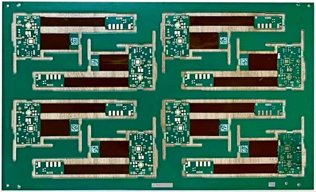
Rigid-Flex PCBs are a hybrid of traditional rigid PCBs and flexible circuits. They incorporate multiple layers of rigid and flexible substrates laminated together into a single board that can maintain shape in some areas while bending in others. This configuration offers design freedom and reliability that rigid or flexible PCBs alone cannot provide.
A typical Rigid-Flex PCB features:
Rigid zones with FR4 material for mechanical strength
Flexible zones with polyimide for bendability
Layered copper traces throughout, sometimes with mixed copper weights
Adhesiveless or adhesive-based bonding techniques depending on use case
These PCBs are ideal for dynamic applications where space-saving, shock resistance, and durability under flexing are critical. Their use reduces the need for connectors and solder joints, thus improving electrical performance and reliability.
Rigid-Flex PCBs are especially beneficial in high-density electronics where three-dimensional (3D) interconnection is needed. Their use allows for innovative product layouts and reduces the total weight and volume of devices.
Rigid-Flex PCBs offer several distinct advantages:
Unlike fully flexible PCBs, Rigid-Flex PCBs maintain mechanical rigidity where needed while still allowing for movement in designated flex areas. This leads to better shock and vibration resistance.
Fewer connectors and shorter interconnect paths improve signal performance and reduce electromagnetic interference (EMI). This is critical in RF, high-speed digital, and analog applications.
By eliminating bulky connectors and allowing more compact folding, Rigid-Flex PCBs save valuable space—an essential factor in mobile, wearable, and aerospace devices.
Solder joints and connectors are common points of failure. Reducing these by using a unified Rigid-Flex PCB results in a more reliable system, especially under mechanical stress or vibration.
The complexity of routing multiple separate PCBs is eliminated. Instead, assembly is streamlined into one integrated board, reducing the bill of materials (BOM) and labor costs.
The fabrication process of Rigid-Flex PCBs is more intricate than that of rigid or flex PCBs alone. It requires specialized equipment and expertise to ensure precision and durability.
Material Preparation
Polyimide and FR4 materials are cut and prepared. Copper foils are laminated to each.
Imaging and Etching
Circuit patterns are created via photoresist and etched chemically to reveal traces.
Layer Lamination
Flexible and rigid layers are selectively laminated. Care is taken to preserve the flexibility in required zones.
Drilling and Plating
Microvias and through-holes are drilled and plated for interconnectivity.
Coverlay and Solder Mask
The flexible parts are covered with a polyimide film (coverlay), while rigid zones receive a solder mask.
Final Surface Finish and Routing
Surface finishes like ENIG or OSP are applied. The board is routed and cleaned.
Testing
Electrical and mechanical tests are performed to ensure integrity.
This high-precision workflow demonstrates why it’s important to work with experienced suppliers such as JM PCB, which specializes in complex Rigid-Flex PCB fabrication.
Choosing the right materials is crucial in ensuring the performance and lifespan of a Rigid-Flex PCB.
Rigid Layers: FR4, High-Tg FR4, Halogen-Free FR4
Flexible Layers: Polyimide (PI), Adhesive or Adhesiveless types
Copper Foils: Rolled Annealed (RA) or Electrolytic (ED) copper
Bonding Films: Acrylic or Epoxy-based adhesives
ENIG (Electroless Nickel Immersion Gold)
OSP (Organic Solderability Preservative)
Immersion Tin or Silver
HASL (Hot Air Solder Leveling)
Material selection directly affects durability under mechanical strain and temperature fluctuations. For mission-critical applications, high-performance materials should always be chosen in consultation with your fabricator.
One of the most critical advantages of Rigid-Flex PCBs is their resilience in extreme environments. Traditional rigid PCBs or flexible-only circuits may fail under thermal stress, vibration, or moisture, but Rigid-Flex PCBs are designed to handle such conditions with superior endurance.
The integration of flexible and rigid zones in a single unified board ensures there are no solder joints or connectors at mechanical transition points. This architecture significantly reduces failure rates caused by thermal expansion and contraction cycles.
In automotive, aerospace, or military electronics, vibration resistance is essential. Rigid-Flex PCBs reduce the number of interconnects and solder joints, minimizing the likelihood of mechanical failure in these harsh conditions. The flexible layers can absorb shocks and mechanical energy better than rigid materials alone.
The polyimide flexible substrates used in Rigid-Flex PCBs are inherently resistant to moisture and chemical degradation. Combined with high-reliability surface finishes such as ENIG, these PCBs are ideal for medical implants, underwater sensors, and outdoor surveillance equipment.
Rigid-Flex PCBs have gained a strong foothold in high-stakes industries due to their compact form factor and robust reliability.
In aircraft systems, where every gram matters and vibration is constant, Rigid-Flex PCBs are used for flight controls, cockpit displays, and navigation modules. Their ability to fit into compact 3D shapes makes them ideal for satellites and unmanned aerial vehicles (UAVs).
Medical equipment such as pacemakers, hearing aids, and surgical tools often require lightweight and compact electronics with excellent mechanical integrity. Rigid-Flex PCBs allow such devices to maintain a small footprint while offering stable electrical performance in high-moisture or bio-sensitive environments.
Defense systems demand the highest reliability and compactness. Rigid-Flex PCBs are used in guidance systems, field radios, and surveillance drones. The shock resistance and long-term durability make them a preferred choice for mission-critical military electronics.
While Rigid-Flex PCBs offer many technical advantages, they are typically more expensive than rigid or flexible boards on a per-unit basis. However, when examined from a system-level perspective, they can lead to substantial cost savings.
Layer count and complexity
Material choice (adhesiveless PI vs adhesive-based)
Surface finish requirements
Tight tolerances and special testing
Design revisions or prototyping cycles
Reduced assembly time due to fewer connectors
Lower failure rates in field use
Compact form factor allows smaller enclosures
Decreased logistics cost due to simplified component count
In many cases, collaborating with a trusted manufacturer like JM PCB early in the design process can significantly reduce development and production costs, particularly through design-for-manufacturing (DFM) consultation.
Designing a Rigid-Flex PCB requires a nuanced understanding of both mechanical and electrical principles. Engineers often make avoidable mistakes that lead to failures or rework.
One common mistake is underestimating the bend radius of the flexible portion. Bending a flex zone beyond its mechanical limits can cause copper cracking and dielectric delamination.
Designers sometimes place vias in areas intended for repeated bending. This can lead to cracking or stress concentration, especially with through-hole plating.
A poorly constructed layer stackup can cause signal integrity issues, mechanical stress, or thermal imbalance. Always consult with experienced fabricators who understand how to optimize stackups for mixed rigid and flexible zones.
Mounting holes, edge clearances, and keep-out zones must be clearly defined to prevent assembly interference or mechanical damage during operation.
Rigid-Flex PCBs are not a universal replacement for all designs, but they do offer distinct advantages over traditional rigid or flexible-only boards when appropriate.
| Feature | Rigid PCBs | Flexible PCBs | Rigid-Flex PCBs |
|---|---|---|---|
| Mechanical Strength | High | Low | High in rigid areas |
| Flexibility | None | High | Controlled flex zones |
| Assembly Complexity | Low | Moderate | Lowest |
| Connector Requirement | Yes | Yes | No |
| Reliability in Harsh Use | Moderate | Moderate | Very High |
| Size Reduction Capability | Limited | Excellent | Excellent |
Use Rigid PCBs for desktop electronics or stationary equipment.
Choose Flexible PCBs for dynamic flexing like foldable displays or wearables.
Opt for Rigid-Flex PCBs when mechanical reliability and space savings are paramount—such as in smartphones, surgical tools, and flight control units.
As this guide has demonstrated, Rigid-Flex PCBs are not just a niche solution—they are a strategic enabler of innovation. Their ability to combine form factor reduction, mechanical flexibility, and electrical reliability makes them essential for next-generation electronics.
From smart wearables to military-grade avionics, Rigid-Flex PCBs provide a foundation for robust and compact product design. While they do require careful design planning and manufacturing expertise, the benefits are far-reaching:
Enhanced product reliability
Simplified assembly and fewer points of failure
Space-saving designs for tightly packed systems
Long-term cost efficiency through failure reduction and system integration
However, leveraging the full potential of Rigid-Flex PCBs requires more than just technical knowledge—it demands the right partnership. With deep experience, fast turnaround, and collaborative engineering, JM PCB remains one of the most trusted and capable manufacturers for projects that demand the best.
Whether you’re building the next life-saving medical device or a rugged drone navigation system, Rigid-Flex PCBs—and the right partner behind them—will shape your path to success.
To help engineers and project leaders better understand the complexities of Rigid-Flex PCBs, here are five frequently asked questions and their expert-level answers:
Q1: What is the difference between rolled copper foil and electrolytic copper foil?
A: Rolled copper foil is produced by mechanically rolling copper into thin sheets, which enhances its ductility, surface uniformity, and mechanical strength. This makes it ideal for dynamic flexing applications. Electrolytic copper foil, in contrast, is deposited from copper sulfate solutions and is typically used where cost is more critical than performance, such as in static flex areas.
Q2: Can Rigid-Flex PCBs be used in RF and high-speed digital applications?
A: Yes. When designed correctly, Rigid-Flex PCBs offer excellent signal integrity. The reduced number of connectors and shorter interconnect lengths result in lower insertion loss and EMI. High-speed designs often incorporate impedance-controlled traces and proper ground referencing across flex zones.
Q3: What’s the typical bend radius required for a Rigid-Flex PCB?
A: The minimum bend radius depends on the thickness of the flex section and the number of layers. A common rule of thumb is:
Single-layer flex: 6x the total thickness
Double-layer flex: 10x the total thickness
Three or more layers: Avoid dynamic bending altogether
Always follow IPC-2223 guidelines or consult with JM PCB to tailor a safe bend design.
Q4: Are there any special storage or handling instructions for Rigid-Flex PCBs?
A: Yes. Rigid-Flex PCBs should be stored in anti-static bags in a humidity-controlled environment (ideally < 50% RH). The flex areas must not be folded sharply during storage or transit. Handling should always be done with ESD-safe gloves and trays to prevent micro-cracking and trace delamination.
Q5: How long is the typical lead time for custom Rigid-Flex PCB fabrication?
A: Lead time can vary depending on complexity:
Simple prototypes (2-4 layers): 7–10 working days
Complex multilayer builds (>6 layers): 12–20 working days
Mass production: Subject to tooling and material procurement, typically 3–4 weeks
JM PCB offers express fabrication options and concurrent engineering support to meet time-critical milestones.


Connect to a Jerico Multilayer PCB engineer to support your project!
Request A Quote


 Quote
Quote