


+86 13603063656
Circuit Board Manufacturing is the cornerstone of the modern electronics industry. From smartphones and smartwatches to industrial control panels and aerospace systems, the humble printed circuit board (PCB) quietly drives nearly every electronic device in existence. Understanding the journey of Circuit Board Manufacturing not only sheds light on the technological sophistication involved but also helps engineers, designers, and business owners appreciate the precision-driven process behind reliable electronic systems.
At its core, Circuit Board Manufacturing involves transforming a blank sheet of insulating material into a fully functional platform where electrical components can communicate efficiently. This transformation is anything but simple. It combines chemistry, material science, mechanical engineering, computer-aided design, and increasingly, automation and artificial intelligence.
This article offers a comprehensive look into the meticulous journey of Circuit Board Manufacturing inside a modern PCB factory. Along the way, it will also share practical insights, personal reflections, and answers to some of the most frequently asked questions in the industry.
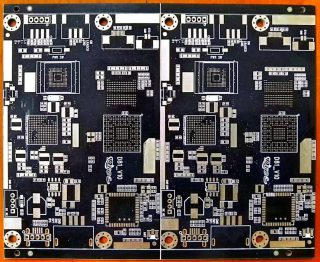
Circuit Board Manufacturing
Circuit Board Manufacturing is not merely an assembly line activity; it is an orchestration of precision processes where each phase demands accuracy and strict quality control. Whether for consumer electronics or mission-critical defense applications, PCB quality can determine the performance and longevity of the final product.
In particular, PCB factories like JM PCB, renowned for their strict adherence to international manufacturing standards, lead the industry by combining technological prowess with scalable efficiency. The company’s multi-tiered quality inspections and vertically integrated supply chain have set a high benchmark in the global PCB landscape.
Understanding the present landscape of Circuit Board Manufacturing requires a glance into its evolutionary history. The idea of mechanically supporting and electrically connecting components dates back to the early 1900s. Initially, point-to-point wiring was the standard method, which quickly became cumbersome and prone to failure as electronic complexity increased.
In 1943, Paul Eisler introduced the first true printed circuit board while working on a radio prototype. Since then, the field has seen quantum leaps—from single-layer PCBs to multilayer, rigid-flex, HDI (High-Density Interconnect), and advanced hybrid substrates.
What was once a manual and experimental endeavor is now a precision-driven, CAD-aided, and automated industry.
The Circuit Board Manufacturing process in a typical PCB factory is divided into several key phases, each integral to the quality of the final board. Below is a detailed look at this workflow:
It all starts with a design—schematics are translated into layout files using EDA software. Before manufacturing begins, the factory’s engineering team performs a Design for Manufacturability (DFM) review to catch any potential issues.
The base material, usually FR4 (a fiberglass-reinforced epoxy laminate), is chosen based on the project’s thermal, electrical, and mechanical needs. Copper foils are laminated onto the core using heat and pressure.
For multilayer boards, inner layers are patterned first. A photosensitive film is applied, UV light is used to define circuit patterns, and then unexposed areas are etched away to leave copper traces.
Multiple inner layers are stacked with prepreg (pre-impregnated resin), aligned, and then pressed together under high heat and pressure to form a single multilayer unit.
CNC machines drill microvias and through-holes with pinpoint accuracy. Laser drills are often used for HDI boards to ensure micron-level precision.
The holes are made conductive by depositing a thin layer of copper through a process called electroless plating. Then, electroplating is done to build up the copper thickness.
The outer layers are processed similarly to the inner layers, with additional layers of copper being patterned to form final circuit paths.
A green (or other color) solder mask is applied to insulate the copper traces and prevent solder bridges during component assembly.
Surface finishes like HASL, ENIG, or immersion silver/gold are applied to pads to ensure solderability and longevity.
Identification labels, logos, and component designators are printed using silkscreening or inkjet methods.
Continuity and isolation tests ensure that every signal path is complete and there are no shorts.
Automated Optical Inspection (AOI), X-ray inspection, and sometimes even manual QC confirm that the boards meet all specifications before they’re vacuum-packed and shipped.
Factories like JM PCB take this process to the next level by integrating MES (Manufacturing Execution Systems) for real-time monitoring and AI-based defect prediction systems to eliminate errors before they occur.
Each step of Circuit Board Manufacturing includes stringent quality control protocols. Key checkpoints include:
DFM and DFA (Design for Assembly) reviews
Lamination alignment and void inspection
Hole wall roughness and aspect ratio evaluation
Solder mask registration and thickness control
Surface finish adhesion testing
100% electrical testing
These measures ensure that the final product meets IPC standards and end-use reliability requirements.
As someone who has closely studied and engaged with PCB production workflows, what strikes me most is the absolute interdependence of each step. A minor misalignment during inner-layer lamination can cascade into signal integrity issues. A poor-quality copper foil can lead to open circuits during reflow soldering.
This deep interconnectivity makes Circuit Board Manufacturing both a science and an art. Watching skilled technicians and sophisticated machines work in harmony inside a facility like JM PCB reveals the hidden complexity behind what the average consumer sees as “just a green board.”
One of the most overlooked yet essential components in Circuit Board Manufacturing is material selection. Every layer, every trace, and every insulating medium contributes to the final performance of the PCB.
The foundation of any PCB is its core material. While FR4 is the most common dielectric material, high-frequency applications might require PTFE (Teflon), polyimide, or ceramic-based substrates. Key considerations include:
Thermal conductivity
Dielectric constant (Dk)
Loss tangent
Moisture absorption rate
High-speed communication PCBs demand low-loss laminates that maintain signal integrity even at frequencies over 10GHz. In such cases, cost often escalates, but the performance benefit justifies the choice.
Copper foil acts as the conductive layer that forms the circuitry. It comes in different thicknesses—usually ½ oz to 2 oz per square foot—and can be rolled or electrolytic.
Smooth copper surfaces are ideal for impedance-controlled traces, while rougher surfaces provide stronger adhesion in power circuitry. The selection here can greatly influence thermal performance and manufacturability.
Prepreg (pre-impregnated resin) is essential in multilayer Circuit Board Manufacturing. It bonds layers together and provides insulation. Different prepreg types vary in resin content and thickness, and improper selection can lead to warping or delamination during lamination.
Modern Circuit Board Manufacturing is no longer just about traditional subtractive etching and drilling. PCB factories like JM PCB have adopted cutting-edge solutions to meet the growing demand for complexity and miniaturization.
Instead of using traditional phototools, LDI projects the circuit pattern directly onto the photoresist using laser beams. It offers micron-level accuracy and is crucial for high-density interconnects.
For multilayer boards, desmearing is essential to remove resin residues from drilled holes, ensuring reliable interlayer connections. Plasma cleaning enhances surface activation and improves copper plating adhesion.
High-layer-count and HDI boards often require sequential lamination to build layers in stages. This process allows for the integration of microvias and buried vias, ensuring better electrical performance and compact layouts.
AOI uses high-resolution cameras and pattern recognition software to detect defects like open traces, nicks, and misalignments. It is integrated after imaging, etching, and solder mask steps to maintain a zero-defect policy.
Sustainability is becoming increasingly important in the electronics industry, and Circuit Board Manufacturing must comply with stringent environmental regulations. PCB factories implement eco-conscious practices, including:
Water recycling and filtration systems
Proper treatment of etchants and plating chemicals
Use of halogen-free laminates
VOC-free solder masks
Factories such as JM PCB take extra steps by adopting green energy initiatives and ISO14001-certified environmental management systems.
With the rise of Industry 4.0, automation plays a pivotal role in reducing human error and improving efficiency. In modern PCB factories, automation includes:
Material handling with robotic arms
Inline inspection and feedback loops
Barcode-based MES tracking for traceability
Real-time process parameter adjustment using AI
This smart manufacturing environment enables JM PCB and similar forward-looking facilities to deliver faster turnaround with improved reliability.
Engineers often encounter several challenges that require close collaboration between the design team and the PCB factory.
Signal integrity is a major concern in high-speed PCBs. Controlled impedance requires precise dielectric thickness, copper width, and consistent material properties. Factories must verify these parameters via test coupons.
Large boards or high-layer-count PCBs are prone to warpage, especially during reflow soldering. Stack-up symmetry, balanced copper distribution, and proper lamination temperature curves help mitigate this issue.
As feature sizes shrink, registration between layers becomes challenging. Optical and X-ray alignment systems ensure drilled holes align precisely with internal pads.
Power-intensive circuits generate significant heat. Incorporating thermal vias, heat spreaders, and metal cores requires precise thermal simulation and careful material selection.
While much of Circuit Board Manufacturing is focused on fabricating the bare board, the final utility lies in its readiness for electronic component assembly. Pre-assembly steps ensure the board is physically, electrically, and chemically compatible with the subsequent soldering and population process.
Different surface finishes serve different assembly techniques. For example:
ENIG (Electroless Nickel Immersion Gold) is ideal for fine-pitch and BGA components.
HASL (Hot Air Solder Leveling) is economical but can result in uneven surfaces.
Immersion Silver and OSP (Organic Solderability Preservative) are environmentally friendly and suited for high-volume applications.
Choosing the right surface finish affects both yield and longevity of the assembled product.
Fiducial markers are critical for SMT pick-and-place machines. These alignment points ensure component accuracy. Tooling holes also help with board orientation during the reflow process.
Before full assembly, thermal profiling is conducted to determine how the board reacts to soldering heat. This is essential for multilayer or metal-core PCBs, which have varying thermal capacities.
Though not always part of a PCB factory’s scope, many advanced facilities—like JM PCB—offer turnkey solutions that include component sourcing and assembly (PCBA). This creates a seamless link between board fabrication and device integration.
SMT is the most common assembly method used today. It includes:
Solder paste printing: A stencil aligns with the PCB and deposits solder paste on pads.
Pick and place: Components are precisely placed on the solder-pasted pads using high-speed machines.
Reflow soldering: Boards pass through a temperature-controlled oven where the paste melts and solidifies, bonding the components.
For components requiring mechanical strength (like connectors), THT is used. Components are inserted into plated holes and soldered either manually or through wave soldering.
Some boards use both SMT and THT, requiring multiple soldering passes. High-layer-count boards or those with sensitive components like MEMS or RF chips demand customized assembly protocols.
After assembly, rigorous testing ensures functionality and reliability.
This checks individual components for shorts, opens, resistance, capacitance, and other values using a bed-of-nails fixture or flying probes.
Simulates the real-world operation of the device. Signals are passed through the board while responses are measured to confirm operational parameters.
These verify solder joint integrity and proper placement, especially for hidden joints like those under BGAs.
In modern electronics, especially wearables, aerospace, and medical applications, flexibility is crucial. Circuit Board Manufacturing must adapt to produce flexible and rigid-flex boards that can endure mechanical stress without failure.
Made of polyimide or polyester substrates
Withstands dynamic bending
Reduced weight and thickness
Requires specialized coverlays instead of solder masks
Combines flexible sections with rigid areas for mounting
Fewer interconnects, reducing failure points
Enhanced mechanical strength
These types require advanced processing, including:
Laser structuring for microvias
Coverlay lamination
3D bend testing and simulation
Factories like JM PCB invest heavily in this niche, offering multilayer rigid-flex production with high-layer counts and advanced bending endurance.
At the final stage of Circuit Board Manufacturing, quality assurance is paramount to ensure customer satisfaction and field reliability.
Despite automation, trained QC personnel still inspect high-value boards under microscopes for:
Cold solder joints
Pad lifting
Surface contamination
Misaligned silkscreen
PCBs are vacuum sealed with desiccants and humidity indicators. Labels include traceability codes, manufacturing dates, and ESD precautions.
Advanced MES systems track every production detail—from material lot numbers to operator logs. Customers receive full reports, including:
Quality certifications (e.g., IPC-A-600 Class 2 or 3)
Electrical test logs
Cross-section micrographs
First Article Inspection (FAI) reports
Circuit Board Manufacturing is undergoing a quiet revolution. Driven by the explosive growth of IoT, 5G, electric vehicles, wearable medical tech, and aerospace systems, the traditional methods of PCB fabrication are being reshaped by automation, data analytics, and sustainability goals.
In this section, we’ll examine where the industry is heading and how forward-looking factories like JM PCB are adapting.
The transformation from traditional manufacturing to a “smart factory” model is among the most significant changes occurring in Circuit Board Manufacturing today.
Artificial intelligence algorithms are increasingly used for real-time defect detection. Cameras capture high-resolution images during AOI or post-etch inspection, and machine learning models detect deviations, predicting potential process drift before defects occur.
Using IoT sensors on equipment such as drill heads, lamination presses, or plating tanks, factories can collect performance data to anticipate maintenance needs—minimizing unplanned downtime.
Manufacturing Execution Systems (MES) and Enterprise Resource Planning (ERP) platforms synchronize:
Material planning
Work order tracking
Operator traceability
Energy consumption
Such integration enhances transparency and customer responsiveness.
Sustainability is no longer optional. Regulatory and corporate social responsibility pressures demand greener processes throughout the entire Circuit Board Manufacturing lifecycle.
Lead-free solders, halogen-free laminates, and water-based solder masks are becoming industry norms. Many customers, particularly in the EU, specify RoHS, REACH, and WEEE-compliant materials.
Etching and plating produce wastewater containing heavy metals. Advanced PCB factories implement closed-loop systems that treat, neutralize, and recycle water for internal reuse.
New formulations of photoresists and solder masks significantly reduce VOCs (volatile organic compounds), protecting both workers and the environment.
Some PCB manufacturers are now publishing carbon emissions data and working toward carbon-neutral facilities by:
Installing solar panels
Using electric forklifts and logistics carts
Offsetting emissions through green certificates
JM PCB, for example, has begun implementing solar-powered processes and digital dashboards to monitor environmental KPIs in real-time.
COVID-19, geopolitical tension, and raw material shortages have highlighted vulnerabilities in the global supply chain that affect Circuit Board Manufacturing.
The price volatility of copper foil and epoxy resins directly impacts board cost and lead times. Manufacturers are mitigating this by:
Establishing long-term supplier contracts
Stockpiling critical materials
Considering alternate suppliers closer to their factories
Even if PCB fabrication is on time, a lack of components can delay final assembly. Some fabricators now offer kitting and partial PCBA services to help customers secure availability earlier.
Cross-border shipping challenges have led many OEMs to prioritize regional or domestic PCB vendors with fast turnaround capabilities. Factories like JM PCB, with global logistics experience, offer air/express/DHL/FedEx options to mitigate time loss.
With the demand for 5G and mmWave communication growing, Circuit Board Manufacturing now incorporates cutting-edge materials.
Materials like Rogers, Isola, and Panasonic Megtron series offer:
Low dielectric loss (Df)
Tight Dk tolerances
Excellent thermal stability
These are essential for high-speed routers, antennas, and radar systems.
High-power applications such as LED lighting and EV inverters require substrates with high thermal conductivity. Metal-core PCBs and ceramic PCBs help dissipate heat effectively.
The trend of embedding capacitors, resistors, or even microcontrollers directly into the board is slowly emerging. This increases board density and reduces parasitic effects.
The journey of Circuit Board Manufacturing is far more than etching copper on fiberglass. It’s a symphony of science, process control, engineering insight, and human coordination.
Whether you’re a startup innovator or a global OEM, your success depends on how well you understand—and collaborate with—the precision world behind your electronics. When you respect the process, align with the factory, and iterate intelligently, your ideas stand a far greater chance of becoming functional, scalable, and extraordinary.
Frequently Asked Questions (FAQs)
Answer: Rolled copper foil is made by mechanically rolling copper into thin sheets, which gives it a smooth surface and high mechanical strength—ideal for flexible circuits. Electrolytic copper foil is formed through electroplating, offering more flexibility and lower cost but with slightly rougher surfaces.
Answer: Reliability is ensured through DFM analysis, real-time monitoring, automated inspections, and strict adherence to IPC class standards. Top-tier factories like JM PCB also invest in predictive maintenance and AI-driven defect tracking systems.
Answer: Common defects include misregistration, delamination, shorts, open circuits, and poor plating. These are prevented through quality material selection, machine calibration, cleanroom practices, and post-process inspections like AOI and flying probe testing.
Answer: Misaligned solder masks can cause exposure of unwanted copper areas, leading to shorts or corrosion. Proper alignment ensures signal integrity and prevents solder bridging during component assembly.
Answer: Surface finish affects solderability, shelf life, and electrical performance. For example, ENIG offers excellent flatness and corrosion resistance, making it ideal for fine-pitch components, whereas HASL is more economical but may not suit HDI designs.


Connect to a Jerico Multilayer PCB engineer to support your project!
Request A Quote


 Quote
Quote