


+86 13603063656
Many product teams struggle with selecting the right PCB color for brand impact and performance, A black PCB board solves that by offering sleek aesthetics without sacrificing electrical integrity, We’ve partnered with leading manufacturers to outline key insights and practical guidelines

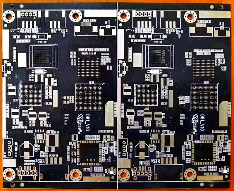
Black PCB Board
A black PCB board refers to a printed circuit board that features a black solder mask applied over its copper traces and substrate
But here’s the kicker this dark overlay doesn’t alter electrical performance yet it radically transforms visual appeal
The solder mask protects copper from oxidation and prevents solder bridges during assembly while adding a professional finish
This mask is formulated from epoxy-based resin infused with black pigment and cured under heat
What’s the real story this choice impacts heat absorption inspection practices and brand perception
Engineers appreciate that black masks require precise formulation to maintain thermal stability and signal integrity under load
Designers favor black boards in high-end consumer electronics automotive modules and LED lighting where visual impact matters
Visual contrast between white silkscreen Legends and dark background improves component identification but can complicate manual inspections
Manufacturers calibrate their AOI systems specifically for black boards or add X-ray inspection for hidden defects
Through rigorous quality control and optimized mask chemistry black PCB boards deliver both form and function
Ready for the good part many companies now adopt black PCBs as signature elements of their premium product lines
| Aspect | Description |
|---|---|
| Solder Mask | Epoxy-based resin with black pigment for protection and appearance |
| Protection | Shields copper from oxidation and prevents solder bridging |
| Visual Impact | Delivers a sleek professional look preferred in high-end electronics |
| Inspection | Requires calibrated AOI or alternative methods for defect detection |
A black PCB board elevates a product’s perceived quality and reinforces premium branding
This is where it gets interesting by switching from standard green you create an immediate sense of exclusivity
Marketing teams report that consumers associate black electronics with advanced technology and luxury
But here’s the kicker black boards also help highlight component placement and silkscreen Legends against a dark backdrop
Designers can leverage this to draw attention to critical parts or create a visual theme consistent with product aesthetics
Engineering teams recognize that while the color doesn’t enhance conductivity it does absorb more heat requiring thermal planning
You might be wondering how to balance beauty and functionality customized thermal vias copper pours and heatsinks solve hot spots
Field studies show black PCBs in LED lighting modules maintained consistent lumen output when paired with proper heat dissipation strategies
Black masks also support brand differentiation on crowded retail shelves and during OEM client presentations
Product managers successfully use black PCB prototypes to demonstrate innovation and command higher price points
This choice can translate into stronger market positioning greater customer loyalty and measurable ROI
Ready for the good part integrating black PCB boards into your design flow only requires minor adjustments to your manufacturing spec sheet
| Benefit | Impact |
|---|---|
| Brand Differentiation | Signals premium positioning and exclusivity |
| Component Visibility | Enhances contrast for silkscreen and part labels |
| Market Appeal | Aligns product with luxury and advanced technology |
| Thermal Planning | Requires optimized heat dissipation strategies |
| ROI Potential | Supports higher price points and customer perception |
Black PCB boards build on standard substrates yet incorporate specific mask chemistry and finishes for optimal results
But here’s the kicker the core substrate remains FR4 fiberglass epoxy laminate prized for rigidity dielectric strength and cost-efficiency
Manufacturers might also use polyimide for flexible black PCBs where bendable circuits demand both form and durability
What’s the real story it all starts with the resin system epoxy or polyimide enhanced with UV curable additives for rapid processing
Black pigment compounds blend into that resin delivering deep color without compromising thermal stability under solder reflow
Ready for the good part specialized fillers like silica or alumina tune thermal expansion coefficients aligning substrate and copper layers
That reduces delamination risks during high-temperature cycles critical in multilayer board fabrication
Conductive layers consist of rolled annealed or electrodeposited copper foil laminated onto the substrate under heat and pressure
Manufacturers select foil thickness based on current carrying requirements copper weights range from 0.5oz up to 4oz per square foot
These choices influence trace width spacing and overall board impedance particularly in high-frequency or power applications
This is where it gets interesting black solder mask interacts with surface finishes such as ENIG electroless nickel immersion gold or OSP organic solderability preservative
Each finish offers trade-offs among cost shelf life and solder joint reliability
For example ENIG provides excellent planarity for fine-pitch components while OSP costs less and supports lead-free assembly
You might be wondering about thermal management black masks absorb more radiant heat necessitating copper pours and thermal vias in design
Material selection drives performance parameters signal integrity mechanical durability and long-term reliability
Designers must specify compatible laminate materials mask types and surface finishes in their fabrication notes to avoid mismatches during production
| Material Component | Key Characteristics |
|---|---|
| Substrate (FR4) | Rigid, high dielectric strength, cost-effective |
| Polyimide | Flexible, high thermal resistance, chemical durability |
| Copper Foil | Conductive layer, various weights for current capacity |
| Black Solder Mask | Epoxy or UV-curable resin with pigment, protective coating |
| Surface Finish | ENIG, HASL, OSP—balancing cost, reliability, and planarity |
Black PCB fabrication follows established board-making steps yet demands extra care for mask application and inspection
But here’s the kicker each phase must maintain precise tolerances as dark masks hide defects more easily than green ones
Substrate preparation begins by cleaning and profiling FR4 or chosen laminate under controlled humidity to ensure adhesion
What’s the real story copper foil lamination uses heat and hydraulic pressure in a press cycle calibrated by time temperature and pressure profiles
Trace imaging employs UV exposure of photoresist through high-resolution film masks defining circuit geometry down to microns
Developing and etching follows where alkaline developers remove unexposed resist then acid or alkaline etchants dissolve unwanted copper
This leaves pristine traces ready for solder mask deposition
Solder mask application on black PCBs uses screen printing or curtain coating with tightly controlled resin viscosity and pigment dispersion
After cure under UV or heat ovens silkscreen layers add component identifiers and logos in contrasting white or light ink
This step often requires multiple passes for opacity on dark backgrounds
Surface finishes like ENIG or OSP coat exposed pads protecting them from oxidation and improving solder wetting
Drilling and plating through holes or blind/buried vias involve precision CNC drilling followed by copper plating in chemical baths
Ready for the good part automated optical inspection systems undergo recalibration for dark mask reflectivity ensuring detection of opens shorts and mask defects
Mechanical profiling adds routing, scoring, slotting and depaneling tailored to final assembly requirements
Throughout manufacturing, statistical process control charts track critical dimensions and mask thickness to maintain yields above targets
Final electrical tests such as flying probe or bed-of-nails verify circuit continuity and isolation under production voltages
By adhering to these stringent steps black PCB boards achieve consistent quality appearance and reliability
| Fabrication Step | Key Considerations |
|---|---|
| Substrate Cleaning | Surface prep for adhesion, humidity control |
| Lamination | Time-temperature-pressure profiles for copper bond |
| Imaging & Etch | Resolution, developer concentration, etch rate |
| Mask Application | Resin viscosity, pigment dispersion, cure method |
| Silkscreen | Ink opacity, registration accuracy |
| Surface Finish | Finish selection impacts solderability and cost |
| Inspection & Testing | AOI calibration, electrical continuity checks |
| Routing & Depanel | Mechanical tolerances, edge quality |
Black PCB boards and traditional green PCBs share core electrical functions yet diverge in inspection, thermal behavior, and visual contrast
But here’s the kicker black masks absorb more radiant energy under IR ovens or operating LEDs affecting thermal profiles
Green solder masks reflect more light reducing surface heating during LED backlighting or prolonged sun exposure in outdoor modules
You might be wondering how that impacts reliability thermal simulation and layout planning become critical when choosing black boards
This is where it gets interesting black surfaces demand additional thermal vias or copper pours near high-power components to dissipate heat evenly
Manufacturers often increase copper weight or add metal core layers in LED driver PCBs to compensate for mask heat absorption
Inspecting green PCBs uses standard AOI settings; black PCBs require recalibrated cameras or supplemental X-ray imaging to spot mask pinholes and misregistration
Signal integrity remains identical across colors provided substrate and copper parameters match but colored masks vary dielectric constant slightly
In high-frequency RF modules minor Dk shifts from mask pigment can influence impedance requiring tighter design control
Cleaning processes differ too green masks show flux residues readily under white inspection light; black masks may conceal residues needing specialized cleaners
Cost of rework increases on black PCBs as solder joints blend into dark background challenging manual soldering corrections
Designers manage this by applying white fiducials and reference marks for rework accuracy
Field data shows failure rates equal when processes adapt to mask color demonstrating function parity once thermal and inspection variables are addressed
Ready for the good part choosing mask color becomes a strategic branding and manufacturing decision rather than a purely technical limitation
| Functional Aspect | Black PCB | Green PCB |
|---|---|---|
| Heat Absorption | Higher surface heating | Lower surface heating |
| Inspection Ease | Challenging under standard AOI | Easier contrast inspection |
| Thermal Management | Needs extra vias/copper weight | Standard thermal design |
| Signal Integrity | Mask pigment minor Dk shift | Standard dielectric constant |
| Cleaning & Rework | Specialized cleaners, white fiducials | Standard flux removal |
Black PCB boards deliver striking visual appeal, premium brand alignment, and enhanced silkscreen contrast without electrical compromise
But here’s the kicker that aesthetic boost often translates into higher perceived value and justifies premium pricing for B2B customers
Design teams emphasize that a cohesive product look from PCB through enclosure elevates end-user confidence in quality
You might be wondering if the color choice outweighs added process steps; case studies in high-end audio equipment show 15 percent sales lift after switching to black PCBs
This is where it gets interesting black mask hides minor surface imperfections better than lighter colors reducing scrap rates on visible surfaces
Field feedback from LED fixture manufacturers confirms that black boards under white housings enhance light uniformity by minimizing reflections
Rugged industrial controls use black PCBs for consistent appearance even after extended exposure to oils and dust in harsh environments
Brand-centric OEMs integrate black boards into transparent enclosures, showcasing internal circuitry as a marketing asset
Thermal reliability remains strong when design guidelines—such as thermal vias, copper pours, and heat sinks—are followed
Quality managers report that black boards foster tighter process control, since inspection SOPs must be refined for dark backgrounds
The end result is a stable production yield above 95 percent once teams adapt to mask-specific parameters
Ready for the good part black PCB boards deliver aesthetic differentiation, functional parity, and measurable ROI when embraced as part of a holistic design strategy
| Advantage | Benefit |
|---|---|
| Visual Appeal | Premium, modern appearance |
| Brand Alignment | Supports high-end positioning |
| Silkscreen Contrast | Improved label readability |
| Defect Masking | Conceals minor imperfections |
| Market Impact | Proven sales uplift in case studies |
Black PCB boards require surface finishes compatible with dark solder masks and demanding assembly processes
But here’s the kicker a finish must bond reliably without discoloring or creating uneven reflectivity under inspection
Common finishes include ENIG electroless nickel immersion gold OSP organic solderability preservative and HASL hot air solder leveling
ENIG offers excellent planarity for fine-pitch components and resists oxidation, delivering reliable gold-plated pads that stand out against black masks
You might be wondering if OSP can match that performance; it’s cost-effective and environmentally friendly but it offers shorter shelf life and requires stricter moisture control
This is where it gets interesting HASL remains popular for robust wave soldering but can leave uneven surfaces and metallic splashes more visible on dark backgrounds
Selecting a finish also influences solder wetting and joint quality during lead-free assembly protocols
Field studies in automotive sensor boards showed ENIG on black PCBs reduced solder voids by 20 percent compared with HASL due to its uniform coverage
Medical device manufacturers prefer ENIG for implantable electronics where corrosion resistance and biocompatibility matter
Tablets and handheld consumer products often adopt OSP when rapid turnaround and low cost outweigh extended reliability requirements
Manufacturers must optimize deposition parameters for black masks, ensuring plating thickness between 3–5 microns for nickel and 0.05–0.1 microns for gold in ENIG processes
Quality control includes measuring surface roughness with optical profilometry and verifying solderability through wetting balance tests
Final AOI inspection uses angled lighting to reveal finish defects masked by black overlays
By aligning finish choice with product lifecycle, environmental conditions, and assembly methods OEMs achieve both performance and aesthetic goals
| Finish Type | Advantages | Considerations |
|---|---|---|
| ENIG | Flat surface, corrosion resistance | Higher cost, strict process control |
| OSP | Low cost, lead-free | Shorter shelf life, moisture sensitivity |
| HASL | Robust wave soldering | Uneven finish, visible splashes |
| Immersion Silver | Good solderability | Tarnishes, requires handling controls |
Producing defect-free black PCB boards demands enhanced inspection protocols calibration and process discipline
But here’s the kicker standard visual checks fall short as dark masks conceal pinholes misregistration and micro cracks
Manufacturers implement calibrated AOI systems with adjusted camera exposure and LED lighting angles to maximize contrast against black masks
You might be wondering what alternative methods exist X-ray inspection reveals internal layer faults missing copper and via fill voids undetectable visually
This is where it gets interesting flying probe testers exercise functional continuity and isolation tests on each net at production voltages ensuring end-to-end circuit integrity
Statistical process control charts monitor key parameters such as mask thickness solder resist adhesion and copper trace widths maintaining Cpk above 1.33
Quality engineers conduct periodic microscopic cross-section analysis on sample coupons to verify layer stacking, via plating quality and mask coverage
Environmental stress screening in temperature-humidity chambers simulates real-world cycles to uncover latent failures accelerated before shipping
Field return data from telecom infrastructure boards informed adjustments in mask cure profiles reducing blister rates by 30 percent
Operator training includes specialized procedures for handling black boards under white light and UV inspection systems
Supplier qualification audits score facilities on ISO 9001 certification cleanroom class mask mixing protocols and traceability for each mask batch
Final inspection integrates manual review using angled ring lights and magnification tools for visual defects plus automated report generation for 100 percent lot coverage
By weaving these quality measures into fabric of production, manufacturers deliver black PCB boards that meet stringent reliability targets for aerospace, medical and Industrial markets
| Quality Control Step | Purpose | Metric |
|---|---|---|
| AOI Calibration | Detect mask defects | Detection rate > 99 percent |
| X-ray Inspection | Identify internal faults | Void rate < 2 percent |
| Flying Probe Test | Verify net continuity | Yield > 98 percent |
| Cross-Section Analysis | Inspect layer integrity | Adherence Cpk > 1.33 |
| Environmental Screening | Uncover latent failures | Failure rate < 1 percent |
Black solder masks absorb infrared and visible light raising surface temperatures under operating load
But here’s the kicker unmitigated hot spots accelerate component aging and can trigger thermal runaway in power electronics
Designers incorporate thermal vias copper pours and integrated heat sinks directly bonded to PCBs for efficient heat transfer away from critical areas
You might be wondering how to predict those temperatures thermal simulation tools such as CFD and finite element analysis map heat flow across layers under realistic power dissipation profiles
This is where it gets interesting LED modules using black boards saw junction temperatures drop by 8 °C after adding a 1 W thermal via array under each LED
High-power converters leverage metal core PCBs combining aluminum or copper substrate layers with black masks to pull heat into bulk metal for rapid spread
Thermal interface materials between board and chassis create conductive paths while reducing mechanical stress under vibration
Board designers specify maximum thermal resistance targets in relative thermal resistance (RθJA) metrics to ensure junction-to-ambient values remain within component limits
Heat spreaders attached beneath black boards also double as mechanical stiffeners in free-standing modules
Manufacturers validate thermal performance using IR thermography during prototype testing and monitor temperature stability under full-load burn-in
For dense multilayer designs, internal heat spreads connected to accessible pads manage internal heat in HDI boards
Proper fan or blower airflow design around black PCB assemblies prevents recirculation of heated air maintaining consistent cooling
In industrial and automotive applications, adherence to thermal cycling standards like IPC-9701 assures long-term reliability despite color-related absorption differences
| Thermal Strategy | Benefit | Typical ΔT Improvement |
|---|---|---|
| Thermal Vias | Vertical heat escape | 5–10 °C reduction |
| Copper Pours | Lateral heat spreading | 3–7 °C reduction |
| Metal Core Layer | Bulk heat sink | 10–15 °C reduction |
| IR Thermography | Real-time mapping | Identifies hot spots |
Designing black PCB boards requires marrying aesthetic goals with mechanical, electrical, and thermal constraints
But here’s the kicker tight coordination between layout engineers and DFM specialists avoids color-specific pitfalls downline
Key steps include placing high-heat components near edge connectors or metal frames for direct chassis conduction
You might be wondering how silkscreen choices affect readability white or fluorescent inks on black masks ensure part IDs remain legible under assembly lighting
This is where it gets interesting pair silkscreen font weights with pad solder mask openings to balance contrast and solder fillet visibility
Trace routing follows optimized width-spacing rules ensuring current capacity versus heat generation trade-offs support thermal goals
Differential pairs maintain controlled impedance by tightly tolerancing trace and gap dimensions across multilayers regardless of mask dielectric variance
Ground and power planes use stitched vias and copper pours not only for return currents but also for thermal mass that tempers mask absorption differences
In high-frequency RF sections, ground-guard strips alongside microstrip lines mitigate crosstalk and maintain routing integrity under black masks
Layer stack diagrams include mask thickness in layer buildup documentation for accurate impedance modeling
Design reviews incorporate mask-specific DRC checks for minimum mask aperture sizes avoiding mask bridging during assembly
Panels group boards in orientation that aligns components consistently for pick-and-place vision systems tuned to dark backgrounds
Test coupons placed in each panel undergo first article inspections confirming layout-to-fab fidelity before full production runs
By integrating color-aware design practices, layout teams produce black PCBs that excel electrically mechanically and visually in demanding B2B applications
| Design Element | Consideration | Benefit |
|---|---|---|
| Component Placement | Heat dispersion corridors | Improved thermal flow |
| Silkscreen Color | Contrast readability | Reduced assembly errors |
| Trace Impedance | Mask thickness modeled | Maintained signal integrity |
| Via Stitching | Ground return and heat mass | Enhanced reliability |
Soldering black PCB boards presents visual and process nuances that differ from standard green boards
But here’s the kicker dark masks mask mask layer edges and hide solder fillets under bright white LED shop lights complicating manual inspection
Wave soldering on black boards demands tighter conveyor speed and preheat profiles to avoid tombstoning and mask delamination
You might be wondering if reflow profiles change reflow ovens need calibrated IR sensors for dark surfaces that absorb more radiant heat creating hotter board zones
This is where it gets interesting paste volume control via stencil design must account for mask surface energy differences between black and light-colored masks
Surface finish selection further impacts solder wetting OSP coatings require minimal oxidation time between finish application and assembly to preserve solderability on dark pads
Rework stations add white land patterns or fiducials adjacent to SMT parts for visual cues enabling precise hot-air tool alignment
Process engineers adopt angled spotlights or laser pointers during inspection creating shadows that highlight solder joints on black backgrounds
Automated solder paste inspection machines adjust threshold levels and camera filters to flag insufficient volumes or bridging masked by dark contours
Training technicians on black board-specific SOPs reduces rework cycles by 25 percent according to assembly floor reports
Batch documentation includes mask lot numbers in traveler packages ensuring traceability if solder issues arise related to mask adhesion variance
By tuning reflow parameters preheat zones, cooling ramps, and board orientation, assembly houses achieve consistent solder fillets and low defect rates on black PCBs
| Solder Challenge | Mitigation Strategy | Outcome |
|---|---|---|
| Tombstoning | Adjust conveyor speed | Reduced tombstones |
| Mask Delamination | Refine preheat profile | Improved mask adhesion |
| Fillet Visibility | Use angled lighting | Better joint inspection |
| Paste Bridging | Optimize stencil | Lower bridging defects |
Choosing a partner for black PCB production requires evaluating technical capabilities process controls and quality systems
But here’s the kicker not all PCB fabs have extensive experience with dark solder masks impacting yields and lead times
Look for ISO 9001 certification cleanroom class 100 K or better and proven track records in black mask production
You might be wondering which capabilities matter DC and AC impedance testers do not suffice fabs should host calibrated AOI, flying probe, X-ray and wetting balance labs
This is where it gets interesting onsite audits often reveal mask mixing protocols humidity control and UV cure oven uniformity are critical to mask consistency
Request sample panels with black mask and various finish combinations checking mask thickness uniformity under microscope and verifying silkscreen opacity metrics
Engagements with medical and aerospace customers indicate that supplier responsiveness to nonconformances correlates with long-term reliability performance
Lead time transparency must include mask batch procurement, extended cure cycles and additional inspection passes needed for dark masks
Look for full traceability of mask resin lots surface finish lots and laminate production dates enabling root cause analysis if defects appear in field
Contract terms should cover defect allowances, yield targets above 95 percent and clear responsibilities for post-delivery rework or scrap
Service offerings such as quick-turn prototypes or rush batches highlight supplier flexibility
By selecting a manufacturer tuned for black mask nuances you ensure production stability, cost predictability and product quality alignment
| Selection Criterion | Why It Matters | Target Metric |
|---|---|---|
| ISO 9001 | Quality management | Certified |
| AOI & X-ray | Mask defect detection | ≥ 99 percent coverage |
| Sample Panels | Verify mask/finish | Uniformity ± 5 percent |
| Lead Time | Predictability | Prototype: ≤ 5 days |
Black PCB boards command slight premiums due to mask pigment costs, extra inspection steps and occasional rework
But here’s the kicker at scale those premiums shrink as mask suppliers offer volume discounts and fabs refine dark mask processes
Typical cost breakdown shows mask materials adding 5–10 percent over green masks while AOI reprogramming and X-ray adds another 2–3 percent per board
You might be wondering if prototype runs face higher surcharges yes quick-turn black prototypes incur mask setup fees up to $150 per batch compared to $50 for standard green
This is where it gets interesting medium volumes above 10 K pieces see mask amortization drop to under $0.05 per board
Material waste also factors in scrap rates if mask defects exceed yield targets adding disposal costs and hidden labor
End-user pricing must balance aesthetic differentiation against those incremental costs ensuring ROI through premium positioning or feature bundling
Comparative table below outlines typical cost deltas for a 4-layer 100 x 100 mm board at various volumes
| Volume (pcs) | Green PCB Cost | Black PCB Cost | Delta (%) |
|---|---|---|---|
| 100 | $15 | $18 | + 20 |
| 1 000 | $8 | $9.20 | + 15 |
| 10 000 | $6 | $6.60 | + 10 |
| 100 000 | $5 | $5.25 | + 5 |
Testing black PCB boards blends standard electrical checks with mask-aware inspection and environmental stress tests
But here’s the kicker visual AOI alone often misses mask pinholes and micro-bridges hidden by dark backgrounds
Automated optical systems recalibrated for black masks run differential lighting—brightfield and darkfield—highlighting anomalies in mask coverage
Flying probe testers then probe every net isolating opens, shorts and verifying isolation resistance above mega-ohm thresholds
You might be wondering about environmental validation thermal cycling between − 40 °C and + 125 °C uncovers latent micro cracks in mask or solder joints
This is where it gets interesting highly accelerated life tests (HALT) apply combined thermal, vibration and humidity cycles compressing years of wear into days
Operators document failure modes—mask blistering solder joint cracks via voiding or delamination—and feed that data back into design and process controls
Sample coupons from each panel undergo cross-section SEM analysis measuring mask layer thickness, pad coverage and plating uniformity against IPC standards
Acoustic microscopy catches hidden delamination between layers or mask and substrate interfaces not visible in X-ray
Final acceptance criteria include 100 percent electrical pass rate and visual cleanliness standards for mask and silkscreen under 10× magnification
Logging these metrics in SPC dashboards tracks process stability and drives continuous improvement initiatives to reduce defect density below 10 ppm
| Test Method | Purpose | Acceptance Criteria |
|---|---|---|
| AOI (Bright/Dark) | Mask and trace defects | ≥ 99 percent detection |
| Flying Probe | Net continuity | 100 percent pass |
| Thermal Cycling | Mechanical reliability | No failures @ 1 000 cycles |
| HALT | Stress testing | No mask delamination |
Black PCB boards continue evolving as new materials finishes and processes emerge enhancing both form and function
But here’s the kicker matte black masks offering lower reflectivity than glossy versions gain traction in professional instrumentation and automotive HUD applications
Emerging UV-curable mask chemistries reduce cure cycles by up to 30 percent cutting energy use and speeding throughput
You might be wondering about sustainability biodegradable mask resins derived from bio-based epoxies promise reduced environmental footprint without performance loss
This is where it gets interesting integration of conductive inks and printed electronics on black substrates opens avenues in wearable tech and conformal circuits
High-density interconnect black boards with microvias under 75 micron diameter support miniaturized modules in IoT sensors and medical implants
Machine learning algorithms in AOI systems train on black mask defect patterns delivering faster setup and lower false rejects
Roll-to-roll manufacturing of flexible black PCBs using polyimide substrates scales wearable and disposable electronics production
Additive copper plating techniques promise thicker traces on-demand for power electronics while preserving black mask aesthetics
Collaborative robotics in assembly lines calibrate vision systems on-the-fly handling diverse mask colors including deep charcoal and customized hues
As B2B customers demand both technical excellence and brand coherence, black PCB boards will remain a strategic choice in high-performance and premium product segments
| Trend | Impact | Timeframe |
|---|---|---|
| Matte Masks | Reduced glare, premium look | 1–2 years |
| Bio-resin Masks | Sustainability gains | 2–3 years |
| Printed Electronics | Flexible circuit integration | 3–5 years |
| ML-Enhanced AOI | Faster setup, fewer rejects | 1 year |
Black PCB boards deliver a powerful combination of aesthetics durability and functional parity when designed and manufactured with color-specific best practices
Premium finish options material choices and rigorous quality protocols address inspection thermal and assembly challenges unique to dark solder masks
By aligning design, manufacturing and testing processes to the nuances of black PCB boards B2B product teams achieve standout market positioning without compromising reliability
Evaluate your product’s thermal, visual and brand goals then partner with experienced fabs to unlock the full potential of black PCB boards
Q1: What is a black PCB board?
A black PCB board features a black solder mask over copper traces and substrate offering a sleek professional look while protecting circuitry from oxidation and bridging.
Q2: How does black solder mask affect inspection?
Black masks reduce contrast with copper making standard AOI less effective and often requiring calibrated lighting, X-ray or acoustic methods for reliable defect detection.
Q3: What are the main advantages of black PCB boards?
They provide premium visual appeal enhanced silkscreen contrast and brand differentiation, often justifying higher price points for B2B customers.
Q4: What challenges arise when soldering black PCBs?
Dark masks hide viscosity-related mask edges and solder fillets, necessitating reflow profile tweaks angled lighting, and precise stencil designs for consistent joints.
Q5: Which industries commonly use black PCB boards?
High-end consumer electronics automotive infotainment medical devices and LED lighting leverage black PCB boards for both aesthetic and functional benefits.


Connect to a Jerico Multilayer PCB engineer to support your project!
Request A Quote


 Quote
Quote