


+86 13603063656

Many engineers struggle when evaluating unpopulated boards What’s the real story They need clarity without getting bogged down in jargon This guide pinpoints the blank PCB concept and its business value By focusing on core definitions and industry usage, you’ll gain confidence in specifying board types Our firm has delivered over a million precision PCBs globally, so you can trust these insights
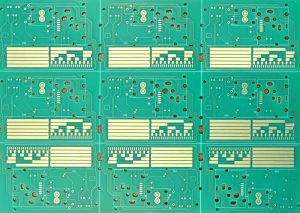
Blank Printed Circuit Board
A blank printed circuit board serves as the foundation of every electronic assembly Unlike populated boards it arrives without components or soldered parts, offering a clean slate for customization But here’s the kicker… blank PCBs already feature etched copper traces drilled holes and solder-mask layers, saving time in early prototyping and production PhD researchers use blank boards when testing novel RF circuits, while startup teams leverage them for rapid design iterations in IoT sensors Automotive R&D departments rely on blank PCBs to validate control module layouts before committing to high-volume runs Each blank board combines mechanical stability with electrical pathways ready for component placement Industrial-grade blank PCBs meet IPC-2221 standards for reliability, whereas hobbyist blanks focus on affordability and ease of use Ready for the good part? major electronics firms reduce development cycles by up to 30% by ordering blanks tailored to layer counts and substrate materials Today’s blank PCBs span single-layer FR-4 sheets, double-layer boards with ground planes, and advanced multilayer cores for HDI applications This versatility ensures seamless integration into assembly lines or bench-top prototyping environments
| Feature | Description | Typical Usage |
|---|---|---|
| Definition | Unpopulated board with copper layers and holes | Prototyping, custom production |
| Layer Counts | Single, double, multilayer | Simple circuits to HDI designs |
| Substrates | FR-4, high-TG, Rogers | Consumer, automotive, RF modules |
| Standards Compliance | IPC-2221, RoHS | Industrial, medical |
| Benefits | Design flexibility, reduced lead time | R&D, low-volume manufacturing |
Engineers begin by transferring a circuit design onto a copper-clad substrate using a photoresist film under UV light. But here’s the kicker… this step defines trace precision and directly impacts yield. After exposure, technicians develop the resist, wash away unexposed regions, and acid-etch the board. This removes unwanted copper while preserving the intended pattern. High-end fabs employ automated spray etchers to achieve consistent edge definition within ±2 microns. Mid-size shops rely on batch etching tanks with controlled agitation to maintain throughput and quality. Effective photolithography sets the stage for reliable connectivity and reduces downstream rework by up to 40%.
| Step | Description | Equipment |
|---|---|---|
| Photoresist Apply | Coat copper surface with light-sensitive polymer | Spin coater |
| UV Exposure | Project pattern from photomask onto board | UV alignment exposure unit |
| Development | Remove unexposed resist to reveal copper underneath | Spray developer |
| Etching | Chemically remove unwanted copper | Spray etcher or tank etcher |
Next, precision drills create holes for component leads and interlayer vias. This is where it gets interesting… modern CNC routers spin carbide bits at speeds exceeding 100,000 RPM to penetrate substrates without delamination. Entry and backing materials protect both board edges and drill bits. Laser drilling tackles microvias under 0.15 mm for HDI applications, enabling next-generation smartphones and high-speed data modules. Each drill hit undergoes optical verification to confirm correct diameter and position within a tolerance of ±5 microns. Utilizing microvia arrays can boost signal integrity in high-frequency boards by 25%.
| Hole Type | Diameter Range | Typical Use |
|---|---|---|
| Through-Hole Vias | 0.3–1.0 mm | Standard component leads |
| Blind/Buried Vias | 0.1–0.3 mm | HDI and multilayer interconnects |
| Thru Microvias | 0.05–0.15 mm | RF modules and compact devices |
Fabricators stack alternating layers of pre-etched cores and prepreg sheets under high heat and pressure. Ready for the good part? this process fuses materials into a rigid, void-free panel. Lamination parameters—temperature up to 190°C, pressure between 400–800 psi, and dwell times of 60–90 minutes—vary by substrate type. Multilayer boards may see five or more lamination cycles to embed ten or more copper layers. Post-lamination, boards undergo cross-sectional inspection to verify bond integrity and dielectric thickness. Proper lamination eliminates delamination risks during solder reflow, ensuring your blank PCB arrives ready for rapid component placement and assembly.
What’s the real story? Choice of substrate determines board durability performance and cost.
FR-4 consists of woven fiberglass cloth infused with epoxy resin offering excellent mechanical strength flame resistance and moderate electrical insulation. Many OEMs favor FR-4 for general-purpose blank PCBs across consumer energy and industrial automation markets. Ready for the good part? advanced variants raise glass transition temperature above 150 °C enabling operation within harsh thermal cycles. Alternative substrates include CEM-1 composites with paper cores for cost-sensitive single-layer boards plus polyimide films prized for flexible or rigid-flex circuit assemblies demanding repeated bending. High-TG laminates and ceramic cores appear when ultra-low expansion minimal dielectric loss and superior heat dissipation matter most.
Copper foil thickness defines conductor current capacity signal integrity and thermal pathways. Standard weight equates 1 oz/ft² (35 µm) accommodating stray currents under 1 A and basic RF traces. Thicker foils at 2 oz or 3 oz (70–105 µm) support high-current power conversion modules and robust heat spreading beneath LEDs or power ICs. This is where it gets interesting… HDI designs often deploy ultra-thin 0.5 oz foils enabling microvia arrays within ten mil trace spacing. Precise copper adhesion onto substrate demands rigorous roll-to-roll lamination controls preventing voids during via plating and solder reflow.
Solder mask shields exposed copper reducing risk of solder bridges corrosion and shorts during assembly. Green remains common due its contrast under AOI cameras while custom hues support branding or functional color-coding in medical aerospace or automotive panels. Silkscreen legends printed using epoxy or acrylic ink identify component locations test points serial data and assembly instructions. But here’s the kicker… silkscreen thickness must balance legibility against pad clearance constraints preventing ink bleed into solderable regions.
| Material Component | Typical Properties | Common Applications |
|---|---|---|
| FR-4 | Tg 130–140 °C Dk ~4.5 mech. strength | Consumer electronics industrial controls |
| Polyimide | Tg 200 °C flexible chemical resistant | Wearables rigid-flex PCBs automotive |
| Copper Foil 1 oz | 35 µm thickness current ≤1 A | Standard signal routing power circuits |
| Copper Foil 2 oz+ | 70–105 µm high current heat spreading | LED backplanes power modules |
| Ceramic | Tg >350 °C low Dk thermal conductor | RF modules aerospace high-power devices |
| Solder Mask | 20–40 µm dielectric insulation | ALL PCB types assembly protection |
| Silkscreen | 10–15 µm ink clear labeling | Component identification regulatory marks |
Blank PCB offerings span single-layer, double-layer, multilayer, and flexible or rigid-flex variants Each type suits particular design demands and production volumes But here’s the kicker… selecting the right blank type upfront saves redesign costs and prevents production bottlenecks
Single-layer blank PCBs arrive with a single copper layer atop an insulating substrate Ideal for low-density circuit deployments they serve LED lighting panels simple sensor interfaces and basic power supplies Budget-sensitive engineers often choose these blanks for pilot runs or proof-of-concept models While single-layer variants shine in cost control they lack the routing flexibility needed for complex signal interactions Consequently they appear mainly in consumer gadgets and entry-level industrial modules
Double-layer blank PCBs feature copper on both sides of the substrate offering enhanced routing pathways and ground plane options This is where it gets interesting… designers leverage through-hole vias to cross signals between layers reducing trace congestion and improving EMC performance Automotive ECU prototypes and compact controller boards frequently use double-layer blanks Their balanced cost versus capability ratio accommodates moderate complexity without the overhead of multilayer manufacturing While slightly more expensive than single-layer blanks they accelerate time-to-market for products requiring moderate feature sets
Multilayer blank PCBs stack three to twelve or more copper layers separated by prepreg sheets delivering ultra-high routing density Ready for the good part? high-density interconnect (HDI) capabilities allow microvias blind and buried vias to populate multilayer blanks supporting next-generation smartphones and advanced telecommunication modules Multilayer blanks incorporate dedicated power and ground planes enhancing signal integrity and thermal management They incur higher lead times and material costs but enable board miniaturization and performance specifications unattainable with fewer layers
Flexible and rigid-flex blank PCBs combine bendable substrates and rigid regions What’s the real story? wearables medical sensors and automotive dashboards exploit flexible blanks for conformal fit and vibration endurance Rigid-flex blanks integrate rigid islands for component mounting linked by flexible tails for connectors or hinges This hybrid approach reduces assembly steps and enhances reliability in constrained enclosures However they demand specialized fabrication controls and incur premium pricing
| PCB Type | Layers | Key Benefits | Typical Applications |
|---|---|---|---|
| Single-Layer | 1 | Lowest cost, fast fabrication | LED panels, simple sensors |
| Double-Layer | 2 | Balanced routing, moderate complexity | Industrial controllers, ECU prototypes |
| Multilayer (3–12+) | 3+ | HDI, power/ground planes, high density routing | Smartphones, telecom backplanes |
| Flexible | 1–4 | Bendable, space-saving, vibration resistant | Wearables, medical devices |
| Rigid-Flex | Hybrid rigid/ | Component support plus flexibility for connectors | Automotive dashboards, foldable electronics |
Rapid prototyping accelerates time-to-market by supplying ready-to-populate boards that already carry copper traces and drilled holes. But here’s the kicker… skipping substrate preparation saves days or weeks in early design cycles. A technology startup testing a new sensor array reduced prototype iterations from five to two by using blank PCBs with predefined stackups. An electronics lab retrofitted its test rigs overnight because blank boards cut fabrication lead time from ten days to three. Manufacturing engineers praise blank PCBs for consistent layer registration and precise drill accuracy, which ensures seamless soldering and reliable first-off yields. This consistency also minimizes troubleshooting overhead and supports concurrent hardware and firmware development across distributed teams.
Blank PCBs let designers tweak layouts without overhauling every fabrication parameter. This is where it gets interesting… swapping component footprints or altering trace routing takes minutes in CAD rather than dozens of hours onsite. An IoT device team replaced a microcontroller footprint three times in one development sprint without ordering new substrates. A robotics OEM iterated motor-control board traces to improve impedance matching for edge sensors, refining performance without altering core manufacturing protocols. That flexibility avoids scrap costs associated with misaligned layers or improper laminate choices. It also simplifies risk management, as supply chain partners handle only one substrate type while assembly partners focus on populated variants.
Small-batch production often faces steep setup charges and minimum order requirements. Ready for the good part? blank PCBs eliminate tooling fees and reduce order quantities to as few as one panel. A medical device prototype run of 25 boards cost 60 percent less when leveraging blank substrates rather than ordering custom-fabricated blanks and assemblies. An aerospace firm trialed avionics control boards without incurring full-volume plating expenses. Bulk procurement of blank substrates also attracts volume discounts, which lowers unit costs when moving from prototyping to pilot production.
| Benefit | Explanation |
|---|---|
| Rapid Prototyping | Cuts fabrication lead time by up to 70% through pre-etched traces and drilled holes |
| Design Iteration Flexibility | Enables multiple layout revisions in CAD without changing substrate specifications |
| Cost Advantages for Small Runs | Avoids tooling fees and supports low-volume orders, reducing prototype run expenses by over 50% |
Selecting correct design rules ensures your blank PCB delivers reliable electrical performance and manufacturing yield
But here’s the kicker… overlooking basic parameters leads to costly rework and delays
Trace Width, Spacing, and Clearance
Trace width dictates current capacity and heat dissipation on a blank Easy PCB. Narrow traces risk overheating when carrying more than rated amps. Many fabs recommend 6 mil minimum for signal traces and no less than 10 mil when currents exceed 1 A. Clearance between adjacent copper features prevents shorts under high-voltage stress. A 6 mil gap suits 50 V circuits, while 10 mil or more is safer for applications above 100 V. Engineers designing automotive control modules found that increasing trace width by 30 percent reduced board temperature by 15 percent in thermal cycling tests.
Impedance Control Basics
This is where it gets interesting… high-speed data lines demand controlled impedance on your blank PCB. Microstrip traces on the outer layer require precise width and dielectric thickness to achieve 50 Ω or 75 Ω targets. Stripline configurations embed signals between ground planes for superior EMI shielding. Designers use time-domain reflectometry (TDR) measurements during prototyping to verify impedance within ±10 percent of target. A telecom OEM reduced bit-error rates by half after switching from uncontrolled to impedance-controlled blank boards.
Thermal Management Strategies
Effective heat management prevents thermal runaway in power electronics built on blank PCBs. Copper pours connected to power planes spread heat across large areas. Thermal vias transfer heat from surface-mounted ICs into internal planes or heat sinks. A lighting manufacturer improved LED lifespan by embedding a 10-via array beneath each emitter, cutting junction temperature by 20 °C. Heavy copper (2 oz/ft²) further enhances conduction for high-power modules. Proper placement of thermal relief patterns around through-holes avoids solder fatigue during reflow.
| Parameter | Recommendation | Purpose |
|---|---|---|
| Trace Width | ≥6 mil (≥10 mil for >1 A) | Safely carry current without excess heating |
| Trace Spacing | ≥6 mil (≥10 mil for >100 V) | Prevent electrical shorts under voltage stress |
| Impedance | Controlled 50 Ω/75 Ω ±10 percent | Maintain signal integrity for high-speed lines |
| Thermal Vias | 6–12 vias per hot component | Channel heat into internal planes or heat sinks |
| Copper Thickness | 1 oz–3 oz/ft² | Balance current capacity with board stiffness |
Selecting the right substrate in a blank printed circuit board dictates electrical behavior thermal resilience and mechanical stability. But here’s the kicker… even subtle substrate variations alter signal speed by up to 30 percent and can trigger board warping under thermal stress. A telecommunications firm tested FR-4 against a high-TG variant for a 5 GHz RF module and found eye-diagram integrity improved 20 percent on high-TG boards during thermal cycling. Meanwhile a medical device startup switched from CEM-1 to ceramic for implantable sensor PCBs and achieved a five-fold reduction in dielectric loss at 10 MHz. Ready for the good part? aerospace suppliers now specify polyimide substrates for flight-control electronics, relying on their 200 °C glass-transition threshold and flexible tolerance under vibration loads that exceed 50 g.
Blank printed circuit boards built on FR-4 deliver balanced cost and performance for general applications while high-TG laminates serve hot-swap power modules in data centers. Ceramic substrates excel in low-loss RF networks found in satellite communications. Designers must weigh dielectric constant which affects impedance calculations signal attenuation and crosstalk. A heavy-equipment OEM discovered that switching to a lower-Dk core reduced cross-talk by 15 db in rugged engine-control PCBs. Mechanical stiffness influences through-hole plating reliability and board flatness. Flexible-core blanks adapt where boards fold around tight chassis features but require thicker copper to offset bending fatigue.
In blank PCB procurement engineers should request substrate datasheets specifying Tg dielectric constant loss tangent coefficient of thermal expansion and moisture absorption rates. That data guides stack-up decisions and informs finite-element thermal simulations predicting hotspot migration under 2 W/cm² heat flux. Case studies show that optimizing substrate choice alone can improve first-pass yields by 25 percent in high-density interconnect (HDI) production runs. When in doubt choose substrates that exceed expected operating conditions. This strategic selection ensures blank printed circuit boards meet reliability targets across consumer automotive aerospace and industrial environments.
| Substrate Material | Tg (°C) | Dielectric Constant (Dk) | Typical Use Cases |
|---|---|---|---|
| FR-4 | 130–140 | ~4.5 | Consumer electronics, general-purpose circuits |
| High-TG Epoxy | 170–200 | ~4.3 | Telecom modules, power electronics |
| Ceramic | 350+ | 9–10 | RF circuits, satellite communications |
| Polyimide | 200–250 | 3.2–3.6 | Flexible assemblies, aerospace, medical devices |
Copper thickness on a blank printed circuit board dictates current capacity heat dissipation and mechanical stiffness But here’s the kicker… even small variations in copper weight can cause voltage drops thermal hotspots or unexpected board flex under load Designers often specify 1 oz copper (roughly 35 µm) for general signal routing and light current demands such as sensor arrays or microcontroller boards. However power modules LED drivers and battery management units frequently require 2 oz or 3 oz copper (70–105 µm) to safely carry several amps without overheating. Field studies at a power inverter manufacturer showed that upgrading from 1 oz to 2 oz copper reduced thermal rise by 25 °C under full load conditions, boosting reliability and extending component lifespans by 15 percent
Thicker copper traces lower electrical resistance enabling blank PCBs to handle higher currents without excessive heat generation. This is where it gets interesting… designers integrate heavy copper planes beneath high-power ICs or MOSFET arrays to serve as heat spreaders. Thermal simulations guide via placement connecting these copper planes to external heat sinks or chassis mounts. A lighting OEM embedded a 12-via array under each 3 oz copper pad and achieved a 30 percent reduction in junction temperature compared to standard copper configurations
Ready for the good part? thicker copper layers increase board rigidity reducing flex during handling or vibration cycles. Aerospace and automotive electronics often specify heavy copper cores for blank PCBs used in engine control modules or flight avionics where boards may endure extreme mechanical stress. These thicker layers also minimize warping during solder reflow cycles maintaining flatness within 50 µm across a 100 mm panel
While heavy copper enhances performance setup costs climb due to longer etch cycles and greater material usage. For low-volume or prototyping runs engineers balance these costs against performance gains. What’s the real story? selecting the correct copper thickness early prevents board revisions and assembly issues downstream
| Copper Weight | Thickness (µm) | Current Capacity (A) | Typical Use Case |
|---|---|---|---|
| 1 oz/ft² | 35 | ≤1 | Signal traces general-purpose PCBs |
| 2 oz/ft² | 70 | 2–4 | Power modules LED drivers |
| 3 oz/ft² | 105 | 4–6 | High-current automotive aerospace PCBs |
| Heavy Copper >3 oz | >105 | ≥6 | Industrial power distribution and busbars |
Vias and holes enable interlayer connectivity component leads and mounting hardware on blank printed circuit boards. This is where it gets interesting… automated CNC drills follow Gerber drill files with micron‐level accuracy drilling thousands of holes per minute without delamination. Entry and backing panels—often aluminum or composite sheets—protect core layers and extend bit life. Laser drilling tackles microvias under 0.1 mm diameter, essential for high-density interconnect (HDI) applications in compact consumer electronics and advanced RF modules. Ready for the good part? plating copper onto via walls transforms bare holes into robust conductors linking surface traces with internal power or ground planes. After drilling, panels undergo electroless copper deposition then electroplating steps to build up thickness within holes, ensuring reliable electrical pathways.
Consider a telecom OEM that retrofitted microvia arrays into existing multilayer cores. By integrating UV laser drilling and sequential copper plating, they boosted interconnect density by 40 percent, shrinking board area and reducing signal crosstalk in a satellite communication module. In another case an industrial controls supplier switched from mechanical drilling to a hybrid laser/blind-via process for a 12-layer power distribution board; this cut stack alignment errors by 25 percent and improved yield under thermal cycling tests. Hobbyist kit manufacturers rely on simple mechanical drilling for through-hole vias, offering low cost but limited to larger component leads and single- or double-layer blanks.
During via formation careful cleaning removes resin smear and debris, preparing holes for plating. Advanced fabs use plasma desmear processes with O₂ or SF₆–based gases to optimize adhesion. Post-plating hole wall roughness promotes solder wicking for through-hole assembly. Quality inspection—often automated optical inspection (AOI) or X-ray analysis—verifies hole size positional accuracy and plating uniformity within ±5 microns tolerance, crucial for high-frequency or high-current boards.
| Via Type | Diameter Range | Drilling Method | Typical Application |
|---|---|---|---|
| Through-Hole | 0.3–1.0 mm | Mechanical CNC Drill | Component leads, mounting hardware |
| Blind Via | 0.1–0.3 mm | Laser or Micro-drill | HDI, signal routing on outer layers |
| Buried Via | 0.1–0.3 mm | Laser | Internal layer interconnects |
| Microvia | 0.05–0.15 mm | UV Laser | High-frequency RF modules |
| Plated Through | — | Electroless & Electro | Multi-layer power and ground connections |
Choosing the correct surface finish on a blank printed circuit board impacts solderability, corrosion resistance, and shelf life But here’s the kicker… the wrong finish can derail assembly yields and introduce field failures
HASL (Hot Air Solder Leveling) remains the most widespread finish thanks to its affordability and robust solderability. Boards pass through a molten solder bath then hot air knives remove excess solder leaving a uniform coating. HASL supports through-hole and surface-mount assembly equally well yet its uneven surface profile challenges fine-pitch components
ENIG (Electroless Nickel Immersion Gold) delivers a flat, gold-plated surface atop a nickel barrier layer. This is where it gets interesting… ENIG resists oxidation indefinitely and provides excellent wire bond capability for RF and high-reliability applications. Aerospace and medical device blanks often specify ENIG despite its premium cost because it prevents black pad defects under aggressive environmental stress
OSP (Organic Solderability Preservative) uses a thin organic film preserving copper until assembly. Ready for the good part? OSP yields ultra-flat surfaces ideal for 0201 and 01005 packages but demands tight control of handling and storage to avoid film breakdown. Consumer electronics prototypes leverage OSP blanks during initial assembly trials before committing to higher-cost finishes
Immersion tin and immersion silver finish variants balance performance, cost, and environmental compliance. Immersion tin offers better wetting than OSP but risks tin whisker formation under certain conditions. Immersion silver avoids whiskers and supports lead-free soldering yet requires stringent surface cleanliness controls. Hard gold plating applies to edge connectors and contact surfaces known for frequent mating cycles
Selecting the right finish for your blank PCB hinges on assembly process, component types, storage conditions, and end-use environment. Integrators working on automotive infotainment frequently choose ENIG for stability under thermal cycling, whereas industrial automation prototypes often use OSP for short-run assembly tests
| Finish Type | Key Properties | Typical Use Cases |
|---|---|---|
| HASL | Cost-effective, resilient solderable | Through-hole, general assemblies |
| ENIG | Flat surface, oxidation-resistant | Aerospace, medical, RF modules |
| OSP | Ultra-flat, lead-free | Fine-pitch SMD prototypes |
| Immersion Tin | Good wetting, moderate cost | Industrial controls, mass production |
| Immersion Silver | Corrosion resistant, flat profile | Consumer wearables, high-volume PCBs |
| Hard Gold Plating | Wear-resistant, solderable | Edge connectors, card slots |
Rigorous testing ensures that blank PCBs meet electrical, mechanical, and environmental standards But here’s the kicker… skipping key tests risks board failures during assembly or in the field
Electrical Continuity testing verifies that all copper traces connect as intended and that no unintended shorts exist. Automated Flying Probe systems probe each node independently, detecting opens and shorts with micron-level precision. These non-contact tests yield fast feedback on prototype panels without requiring custom test fixtures. Manufacturers often report first-pass yields above 98 percent when incorporating flying probe checks early in production
Automated Optical Inspection (AOI) employs high-resolution cameras to scan blank PCBs for defects such as missing copper, over-etch, drill debris, and solder mask mis-registration. This is where it gets interesting… dual-camera AOI setups capture top and bottom layers simultaneously, cutting inspection time in half while maintaining sub-10-micron detection thresholds. Many fabs use inline AOI directly after etching and after solder mask application to catch errors before costly lamination or plating steps
X-Ray Inspection complements AOI for multilayer blanks by imaging internal copper and via structures. Faulty via fill, delamination, or cross-layer shorts reveal themselves under X-ray, enabling corrective action before board completion. Data shows incorporating X-ray yields 30 percent fewer internal defect escapes in high-density interconnect (HDI) runs
Environmental Stress Screening subjects blanks to thermal cycling between –40 °C and 125 °C, humidity soak, and vibration. Extended exposure uncovers delamination, substrate cracks, and adhesion failures. Ready for the good part? boards that survive 100 thermal cycles with no layer separation earn premium reliability status for automotive and aerospace programs
| Test Method | Purpose | Detection Capability |
|---|---|---|
| Flying Probe Continuity | Verify opens/shorts | ±10 µm |
| AOI (Optical Inspection) | Surface defect detection | ≥5 µm missing copper, mask faults |
| X-Ray Inspection | Internal layer and via integrity | Via fill voids, internal shorts |
| Thermal Cycling | Delamination and adhesion testing | –40 °C to 125 °C, 100 cycles |
| Vibration Testing | Mechanical resilience | Up to 50 g acceleration |
Adhering to industry standards ensures blank PCBs perform reliably across applications But here’s the kicker… non-compliant blanks introduce assembly failures and warranty returns
IPC-2221 outlines generic design rules such as trace width, spacing, and pad geometry. Designers reference IPC-2221 when creating Gerber files for blank PCBs to meet minimum electrical clearance under specified voltages. Compliance reduces scrap rates and accelerates board approval cycles
IPC-6012 defines qualification and performance specifications for rigid PCBs. Performance classes (1–3) cover climatic exposure, electrical cycling, and mechanical stress. This is where it gets interesting… performance class 3 blanks meet the most stringent automotive and aerospace requirements, enduring accelerated thermal cycling and moisture exposure without degradation
RoHS (Restriction of Hazardous Substances) compliance limits lead, mercury, cadmium, and other toxins in materials and finishes. Many blank PCB substrates and finishes require third-party testing and a declaration of compliance before export to EU or global markets. Failing to demonstrate RoHS compliance blocks boards from assembly lines in regulated industries
UL 94 flammability ratings classify substrate materials based on burn rates under direct flame exposure. Blank PCBs built for industrial panels often specify UL 94 V-0 or V-1 ratings for safety in power distribution equipment
ISO 9001 certification indicates a manufacturer’s quality management system meets global best practices. While not PCB-specific, ISO 9001 ensures process controls, document traceability, and continual improvement frameworks within the fabrication facility
| Standard | Scope | Applicability |
|---|---|---|
| IPC-2221 | Design rules for geometry and spacing | All rigid blank PCBs |
| IPC-6012 | Performance and reliability classes | Automotive, aerospace, medical |
| RoHS | Restricted hazardous substances | EU and global electronic goods |
| UL 94 | Flammability classification | Power panels, industrial boards |
| ISO 9001 | Quality management systems | Fabricators and supply chain |
Blank PCB costs hinge on substrate, layer count, copper weight, and finish But here’s the kicker… small changes in spec can spike pricing by 30 percent
Material costs ascend with TG rating and specialty substrates. FR-4 remains the baseline at $2–$5 per ft² for single-layer blanks. High-TG laminates command $6–$12 per ft², while ceramic cores can exceed $20 per ft² for low-loss RF applications. This is where it gets interesting… polyimide-based blanks start at $10 per ft² but justify their premium in flexible and rigid-flex scenarios
Layer count adds lamination, drilling, and inspection complexity proportionally. Each additional layer incurs $1–$3 per layer premium. A four-layer blank may cost $8 per ft² while a ten-layer HDI core can approach $30 per ft². Early design teams simulate board performance to right-size layer counts before incurring stacking fees
Copper weight influences etching cycle times and material usage. Standard 1 oz copper adds no surcharge, but 2 oz and 3 oz foils increase costs by 15 and 30 percent respectively. Heavy copper lanes drive power module reliability but weigh on budgets if over-specified
Small-batch orders often face volume surcharges due to setup fees and warehousing costs. Many fabs waive tooling for runs above 50 panels but impose $100–$300 tooling charges for sample lots under ten units. Consolidating orders across product variants can dilute setup expenses
| Cost Factor | Impact on Price | Cost Range |
|---|---|---|
| Substrate Type | Base material cost | $2–$20+ per ft² |
| Layer Count | Lamination and drilling fees | $1–$3 per additional layer |
| Copper Weight | Material surcharge | +15–30% for 2–3 oz foils |
| Surface Finish | Finish process cost | $0.10–$1.00 per ft² |
| Order Quantity | Setup and tooling fees | Waived above 50; $100–$300 |
Blank PCBs underpin prototypes across industries Ready for the good part? they accelerate innovation cycles without committing to full assemblies
Consumer electronics startups test single-layer blanks for wearables, smartphone interface modules, and IoT sensors. These quick-turn blanks support rapid code-hardware integration and real-world beta trials within weeks
Industrial automation firms rely on double-layer blanks to validate PLC boards, motor drivers, and sensor arrays. The moderate complexity blanks allow embedded developers to debug ladder logic and firmware concurrently with PCB assembly
Automotive OEMs employ multilayer blanks for engine control units (ECUs), infotainment modules, and ADAS sensors. High-TG blanks resist under-hood thermal loads while rigid-flex prototypes validate infotainment screen hinges and antenna arrays
Medical device innovators select ENIG-finished blanks for patient monitoring systems, infusion pumps, and imaging probes. Strict IPC and UL standards ensure biocompatibility and reliability in sterile environments
Telecom and RF specialists integrate ceramic blanks within satellite transceivers, radar arrays, and 5G base station modules. Low-loss substrates enable signal fidelity at multi-GHz frequencies critical for modern wireless networks
| Industry | Blank PCB Type | Key Benefits |
|---|---|---|
| Consumer Electronics | Single-layer OSP | Fast prototypes, low cost |
| Industrial Automation | Double-layer FR-4 | Balanced functionality and price |
| Automotive | Multilayer high-TG | Thermal resilience, HDI connectivity |
| Medical | ENIG-finished FR-4 | Sterile compliance, solderability |
| Telecommunications | Ceramic low-loss | High-frequency performance |
Choosing a reliable supplier ensures your blank PCBs arrive on spec and on time What’s the real story? partner vetting saves weeks of delays and warranty headaches
Evaluate manufacturing capabilities by reviewing equipment lists for photolithography, CNC drilling, and lamination presses. Suppliers with automated AOI and X-ray systems flag defects early enhancing first-pass yield
Compare lead times and minimum order quantities. Some fabs promise prototype blanks within 3–5 days while others require 10–14 days setups. MOQ policies vary from single-panel trials to batches of 25 units. Balancing speed and cost hinges on your development schedule
Assess pricing structures transparently. Look for line-item breakdowns covering substrate, lamination, drilling, plating, and finish. Hidden fees surface in express routing or rework services—clarify these before signing purchase orders
Verify quality certifications such as IPC-A-600 class ratings, ISO 9001 quality management, and UL or RoHS declarations. Quality systems indicate consistent process control and compliance with global standards
Engage customer support through technical inquiries. Responsive engineers who advise on stack-ups via free DFM reviews signal robust support infrastructure. Ask for sample panels to evaluate physical attributes firsthand before scaling to production
| Selection Criterion | Key Questions | Acceptable Threshold |
|---|---|---|
| Equipment | Does the fab offer laser drilling and AOI? | Automated AOI, UV laser capability |
| Lead Time | Prototype delivery turnaround time | ≤5 days for standard blanks |
| MOQ | Minimum sample order requirement | 1–5 panels |
| Pricing Transparency | Are all process costs clearly itemized? | No hidden fees |
| Certifications | IPC, ISO 9001, RoHS, UL compliance | Verified certificates |
| Technical Support | Availability of DFM reviews and response time | ≤24-hour technical response |
Q1: What is a Blank Printed Circuit Board?
A blank printed circuit board is an unpopulated board substrate with etched copper traces and prepared holes, ready for component assembly
Q2: How does blank PCB manufacturing work?
The process involves layer lamination, photolithographic copper patterning, chemical etching, drilling, plating, and surface finishing steps
Q3: What materials are used in blank PCBs?
Common materials include FR-4, CEM-1 composites, high-TG laminates, copper foil, solder mask polymers, and silkscreen inks
Q4: What standards apply to blank PCB fabrication?
Key standards include IPC-2221 for design rules, IPC-6012 for performance specs, plus RoHS and UL certifications for safety and environmental compliance
Q5: How do I choose a blank PCB supplier?
Assess their technical capabilities, lead times, minimum order quantities, pricing structure, quality certifications, and customer support offerings


Connect to a Jerico Multilayer PCB engineer to support your project!
Request A Quote


 Quote
Quote