


+86 13603063656
Copper PCB boards are the foundation of today’s high-performance electronics. Whether you’re designing power converters, electric vehicle systems, or industrial machinery, copper-based PCBs offer unmatched current-carrying capacity and thermal performance. But here’s the kicker… not all copper PCBs are created equal. The type of copper, its thickness, and how it’s implemented in your board’s design can drastically affect efficiency, durability, and cost. In this comprehensive guide, we’ll walk through everything B2B engineers, buyers, and OEMs need to know about copper PCB boards—from technical specifications and materials to production, pricing, and future innovations.

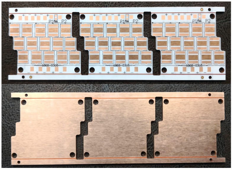
Copper PCB Board
Copper PCB boards are printed circuit boards that use copper layers to create conductive paths for electricity. They’re prized for their ability to carry high current and dissipate heat efficiently—two crucial features in today’s power-hungry and thermally demanding applications.
But what’s the real story? It’s not just about slapping copper on a board. Engineers choose copper PCBs for their durability, reliability in harsh environments, and ability to reduce power losses. These boards are used in everything from smartphones and servers to solar inverters and military-grade devices.
And for B2B manufacturers, the right copper PCB can mean fewer product returns, better performance under load, and longer device lifespan. That’s why understanding the nuances of copper PCB types, materials, and processing methods is essential.
| Industry | Common Use Cases |
|---|---|
| Power Electronics | Power converters, transformers |
| Automotive | EV battery systems, control modules |
| Renewable Energy | Solar inverters, wind turbine controllers |
| Aerospace & Defense | Radar, avionics, high-load control systems |
| Industrial Controls | PLCs, motors, robotics, automation systems |
Copper is the metal of choice for PCB traces because of its superb electrical and thermal conductivity. It allows signals to travel with minimal resistance and dissipates heat efficiently, reducing the risk of hot spots and damage.
Ready for the good part? Copper’s conductivity (around 5.96×10⁷ S/m) is only slightly lower than silver—but much more cost-effective. Its thermal conductivity also makes it ideal for heat-sensitive applications like LED lighting or RF modules.
Additionally, copper’s ductility makes it easy to etch into fine traces for compact designs while supporting high current loads in power-intensive circuits. Whether you need microstrip lines for signal fidelity or wide power buses for industrial loads, copper is king.
| Property | Value |
|---|---|
| Electrical Conductivity | 5.96×10⁷ S/m |
| Thermal Conductivity | 401 W/m·K |
| Density | 8.96 g/cm³ |
| Melting Point | 1,085°C (1,984°F) |
| Tensile Strength | 210 MPa (annealed copper) |
Not all copper PCBs are the same. The application determines whether you need standard, heavy, or ultra-thick copper—and that decision affects everything from etching to performance to cost.
Standard copper PCBs use 1 oz/ft² or 35μm copper and are used in most consumer electronics. But here’s where it gets interesting… Heavy copper PCBs (3 oz/ft² to 10 oz/ft²) are engineered for power electronics, while ultra-thick copper PCBs (above 10 oz/ft²) serve high-current environments like power supplies or welding equipment.
You’ll also find single-sided copper PCBs, double-sided boards for more routing freedom, and multilayer copper PCBs used in telecom, defense, and data centers.
| Type | Copper Thickness | Applications |
|---|---|---|
| Standard Copper | 1 oz/ft² | Consumer electronics, LED drivers |
| Heavy Copper | 3–10 oz/ft² | Power modules, automotive relays |
| Ultra-Thick Copper | 10–20 oz/ft² | Industrial controls, power buses |
| Multilayer Copper PCB | Varies by layer | Servers, EVs, military systems |
| Double-Sided PCB | 1–4 oz/ft² | Control systems, sensors |
Let’s break down what makes up a copper PCB. At the core, you’ll find a substrate—typically FR4 for standard applications, or high-Tg, aluminum, or ceramic for extreme environments. Laminated over this substrate is the copper foil.
But here’s the kicker… copper foil comes in multiple grades: ED (Electrodeposited) for general use and RA (Rolled Annealed) for flexible boards that require durability under bending.
Add in solder mask to protect traces, and surface finishes like HASL, ENIG, or OSP to ensure solderability. For high-power or high-frequency PCBs, thermal vias, heat sinks, and insulating materials are integrated to support the board’s workload.
| Material Component | Options Available | Use Case |
|---|---|---|
| Substrate | FR4, High-Tg FR4, Aluminum, Ceramic | Standard vs. high-heat boards |
| Copper Foil | ED, RA, Thickness 1–20 oz/ft² | Current-carrying optimization |
| Solder Mask | Green, Black, White, Blue | Insulation and appearance |
| Surface Finish | HASL, ENIG, OSP, Immersion Silver | Solderability and shelf life |
Copper thickness is more than just a number—it’s a direct influencer of electrical and thermal behavior. But here’s the real story… choosing the right copper weight can mean the difference between flawless performance and overheating failure.
Thickness is measured in ounces per square foot (oz/ft²). 1 oz equals 35μm thickness. Higher copper weights can carry more current but are harder to etch, increasing manufacturing complexity and cost.
Use 1 oz copper for signal processing or consumer devices. Step up to 2 oz or 3 oz for power electronics. Ultra-thick layers (10 oz+) are used in DC-DC converters, motor drivers, and renewable systems.
| Copper Weight | Thickness (μm) | Max Current (via 10mm trace @ 10°C rise) |
|---|---|---|
| 1 oz/ft² | 35μm | ~5.8A |
| 2 oz/ft² | 70μm | ~9.8A |
| 3 oz/ft² | 105μm | ~13.8A |
| 10 oz/ft² | 350μm | ~35A+ |
Designing a copper PCB isn’t just about drawing traces—it’s a fine art of balancing current flow, thermal control, and manufacturability. And this is where it gets interesting… as copper weight increases, so do the spacing requirements, etching tolerances, and design challenges.
First, consider trace width. Higher current means wider traces. For instance, a 2 oz copper board may need double the trace width of a 1 oz board to carry the same current without overheating. Use IPC-2221 standards as a guideline for trace width and spacing based on current load and copper weight.
Via design is also critical. For thick copper layers, use multiple vias or larger plated through holes to handle current transfer between layers. For multilayer copper PCBs, layer stack-up must be carefully designed to avoid thermal imbalance or warping.
Also, always confirm with your manufacturer’s capabilities for minimum trace/space and copper plating limits to avoid overdesigning a board that’s impossible to fabricate.
| Copper Weight | Minimum Trace Width | Minimum Spacing | Via Diameter |
|---|---|---|---|
| 1 oz/ft² | 6 mil | 6 mil | 0.3 mm |
| 2 oz/ft² | 10 mil | 10 mil | 0.4 mm |
| 3 oz/ft² | 14 mil | 14 mil | 0.5 mm |
| 10 oz/ft² | 24 mil | 24 mil | 0.8 mm |
So why do B2B buyers choose copper PCB boards over other alternatives? The answer lies in performance—and we’re not just talking about better conductivity. Copper PCBs offer three major advantages: current handling, thermal management, and long-term reliability.
Here’s the real story… copper’s low resistivity minimizes voltage drop across the board, making it ideal for high-current paths. Thick copper spreads heat evenly, protecting components from thermal stress. And because copper resists corrosion and fatigue, it extends PCB life in harsh operating environments.
From high-speed data transmission to electric vehicle battery management systems, copper PCBs are trusted because they hold up under pressure—literally and electrically.
| Feature | Benefit |
|---|---|
| High Conductivity | Reduces power loss |
| Excellent Heat Dissipation | Protects components, enables fanless design |
| High Mechanical Strength | Withstands shock, vibration, and load |
| Long Lifecycle | Reduces need for replacements/repairs |
| High Current Support | Enables heavy-duty power applications |
Copper PCB boards are everywhere high current, heat, or precision control is required. But what’s the real story? Their ability to handle harsh loads and environments makes them indispensable in today’s high-tech world.
In automotive, they’re used in power steering, brake systems, and battery management units. In renewable energy, they manage DC-DC conversion and inverter output. In telecom, they help regulate power distribution for base stations and servers.
They also find application in industrial machinery, from motor drivers to programmable logic controllers (PLCs), and even military electronics, where reliability is mission-critical.
| Industry | Example Use Case |
|---|---|
| Automotive | EV chargers, BMS, lighting controllers |
| Renewable Energy | Solar inverters, wind controllers |
| Telecom | Power amplifiers, base station filters |
| Industrial | Servo drivers, CNC control boards |
| Aerospace | Radar power systems, avionics backplanes |
Now, let’s step into the factory. Manufacturing a copper PCB board is a high-precision process that must account for copper weight, board thickness, and etching detail. And here’s the kicker… heavier copper makes nearly every process step more complex.
It begins with laminating copper foil onto the dielectric substrate. Next, photoresist is applied and exposed to define trace patterns. Etching then removes unwanted copper—this is more difficult with thick copper, requiring slower etch rates and higher chemistry control.
Afterward, drilling and plating create vias, followed by solder mask application, silkscreen printing, and surface finish plating like ENIG or HASL. The final steps are electrical testing and AOI before packaging.
| Stage | Description |
|---|---|
| Lamination | Bonding copper to substrate |
| Imaging & Etching | Creating the circuit traces |
| Drilling & Plating | Making vias conductive |
| Mask & Finish | Applying protective layers and finish |
| Testing & Inspection | Ensuring quality and circuit functionality |
What sets copper PCBs apart? Let’s put them head-to-head with other types like aluminum and standard FR4 boards. And here’s where it gets interesting… copper PCBs combine the strength of aluminum with the design flexibility of multilayer FR4.
Aluminum PCBs are good at heat dissipation but not ideal for multilayer or high-speed circuits. Standard FR4 PCBs are cheaper but don’t perform well in high-current or high-temp environments.
When you need both power and precision—copper is the go-to.
| PCB Type | Thermal Conductivity | Cost | Multilayer Capability | Typical Use |
|---|---|---|---|---|
| Copper | Excellent | Medium–High | High | Power, industry |
| Aluminum | Good | Low–Medium | Limited | LEDs, basic lighting |
| FR4 Standard | Poor | Low | High | Consumer electronics |
In high-power and high-stakes industries, testing a copper PCB board is not optional—it’s essential. But here’s the real story… when copper thickness increases, so does the importance of detailed quality checks.
The testing process begins with automated optical inspection (AOI) to identify visual flaws like solder bridges, trace gaps, or misalignments. Then comes electrical testing, where every net on the board is verified for continuity and insulation resistance.
For heavy copper PCBs, thermal stress testing is crucial. Boards are subjected to temperature cycling to evaluate how well they manage heat and resist delamination. In mission-critical fields like aerospace and defense, X-ray and CT scanning are used to inspect internal vias and solder joints.
| Test Type | Purpose | When Used |
|---|---|---|
| AOI | Surface defect detection | All copper PCBs |
| Flying Probe | Net continuity for low volumes | Prototypes, low batch |
| Bed of Nails (ICT) | Electrical connectivity at high speed | Mass production |
| Thermal Cycling | Heat resistance validation | Automotive, energy, defense |
| X-Ray/CT Inspection | Hidden voids or internal joint issues | Military, aerospace |
Producing copper PCBs—especially heavy copper types—is no walk in the park. And this is where it gets interesting… the very things that make copper PCBs desirable also introduce fabrication complexity.
First off, etching thick copper is harder. It requires slower rates and more chemicals, which can cause undercutting or uneven trace edges. Then there’s thermal management during lamination—thick copper conducts heat away fast, so precise thermal profiles are needed.
Heavy copper also introduces mechanical stress during drilling and plating. If the process isn’t tightly controlled, delamination, warping, or plating voids can occur—especially in multilayer boards.
| Challenge | Cause | Solution |
|---|---|---|
| Uneven Etching | Thick copper requires slow etch rates | Controlled etching chemistry |
| Warping or Curling | High copper weight + poor lamination | Even copper distribution |
| Via Wall Plating Issues | Deep holes in thick boards | Step plating or filled vias |
| Delamination | Rapid heat expansion or poor bonding | High-Tg materials, vacuum lamination |
Let’s talk money—because copper PCB boards aren’t the cheapest option out there. But here’s the kicker… understanding what drives cost can help you optimize your design and order strategy.
The biggest pricing factor? Copper weight. The thicker the copper, the higher the material and processing cost. Board size, layer count, and drill complexity also add up quickly. Surface finish choices like ENIG or Immersion Silver are pricier but offer better performance.
And don’t forget about volume pricing—larger batches reduce per-board cost due to amortized setup fees. Prototyping with 1–2 oz copper and scaling to heavy copper for production is a cost-efficient strategy.
| Factor | Impact Level | Optimization Tip |
|---|---|---|
| Copper Weight | High | Use only where needed |
| Number of Layers | Medium | Simplify layout if possible |
| Surface Finish | Medium | Choose based on assembly needs |
| PCB Size & Thickness | High | Panelize small designs when possible |
| Volume Order | Very High | Consolidate orders for better pricing |
Let’s face it—choosing the right PCB supplier can make or break your project. This is especially true for copper PCB boards, where expertise, equipment, and certifications matter more than ever.
But what’s the real story? Not all PCB manufacturers are capable of producing heavy or ultra-thick copper PCBs. Look for suppliers with proven experience, IPC/ISO/UL certifications, and in-house DFM support. Request samples and verify consistency in copper plating and etching.
Also, ask about their AOI, thermal test, and plating inspection capabilities. A vendor that invests in advanced inspection ensures better quality and fewer returns. Finally, assess their logistics and export compliance—especially if you’re ordering internationally.
| Criteria | Importance Level | What to Ask |
|---|---|---|
| Heavy Copper Experience | Critical | Request examples or case studies |
| Certifications (IPC, UL, ISO) | High | Verify documents and audit reports |
| DFM & Engineering Support | High | Do they help optimize your design? |
| Quality Control Tools | Very High | Do they use AOI, X-ray, thermal testing? |
| Export Compliance & Logistics | Medium–High | Can they handle global shipments, DDP? |
So, what’s next for copper PCB boards? The demand is only growing. But here’s the kicker… innovation is happening across materials, design, and processing.
High-frequency copper PCBs are now in demand for 5G, radar, and satellite applications. New laminates like PTFE composites and low-loss resins are paired with thick copper for both speed and power.
There’s also a push for sustainable PCB production, with eco-friendly etchants, water-saving rinsing systems, and recyclable laminates. Embedded components and copper-polymer hybrids are becoming mainstream to reduce size and boost performance.
And of course, the rise of EVs and renewable energy will keep driving demand for heavy copper PCBs that can handle energy conversion at scale.
| Trend | Industry Impact |
|---|---|
| Copper for 5G & High-Speed | Data centers, aerospace, telecom |
| Eco-Friendly Processing | Consumer electronics, automotive |
| Embedded Passive Components | Miniaturization in IoT and mobile devices |
| EV Power Converters | Electric vehicles, charging stations |
| Copper-Polymer Hybrid PCBs | Wearables, flexible circuits |
Q1: What is a copper PCB board?
A copper PCB board is a printed circuit board that uses copper layers as the conductive material for electrical signal paths, known for excellent conductivity and heat dissipation.
Q2: How does copper affect PCB performance?
Copper enhances current-carrying capacity, lowers resistance, improves heat distribution, and supports high-reliability applications in power, automotive, and industrial sectors.
Q3: What is heavy copper and when is it used?
Heavy copper refers to PCBs with copper layers thicker than 3 oz/ft². They’re used in power supplies, motor drivers, and EV systems to support high currents and temperatures.
Q4: Can copper PCBs be multilayered?
Yes, copper PCBs can be single, double, or multilayer. Multilayer copper boards are used for complex routing, power distribution, and electromagnetic shielding in advanced electronics.
Q5: Are copper PCBs more expensive than regular PCBs?
Yes, copper PCBs are generally more expensive due to higher material costs, more complex processing, and additional quality control—especially for heavy or ultra-thick designs.


Connect to a Jerico Multilayer PCB engineer to support your project!
Request A Quote


 Quote
Quote