


+86 13603063656
Copper PCB boards are a critical component in many electronics, offering superior electrical conductivity and heat dissipation capabilities. In this article, we’ll delve into the benefits, manufacturing processes, and applications of copper PCB boards. By the end, you’ll understand why copper is often the material of choice for high-performance electronics and how to incorporate it into your designs.

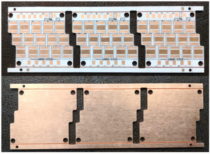
PCB boards
Copper PCB boards are printed circuit boards that use copper as the primary conductive material. Copper’s excellent electrical conductivity makes it an ideal choice for many high-performance and high-power applications. Unlike traditional PCBs made with aluminum or other materials, copper PCBs ensure optimal signal transmission, minimal heat buildup, and greater durability.
But here’s the kicker – copper’s benefits go beyond just conductivity. Copper PCBs also provide superior thermal management, ensuring that high-energy components do not overheat during operation. This makes copper PCBs perfect for use in power electronics, automotive devices, and other high-demand applications.
Copper PCBs come in different forms, such as single-sided, double-sided, and multilayer boards. The thickness of the copper used in these boards can vary depending on the power handling and thermal requirements of the device. In some applications, especially in power supplies, thicker copper layers are used to handle the increased current.
| Type of PCB | Applications | Benefits | Common Copper Thickness |
|---|---|---|---|
| Single-Sided | Basic electronics | Simple design, cost-effective | 35µm – 70µm |
| Double-Sided | Power electronics, consumer devices | More complex designs, space-saving | 70µm – 105µm |
| Multilayer | High-frequency circuits, servers | High-density, better heat dissipation | 105µm – 200µm |
Copper offers several advantages over other materials used for PCBs, like aluminum and FR4. One of the key benefits of copper PCBs is their excellent electrical conductivity. Copper allows for efficient signal transmission with minimal losses, which is crucial for high-frequency applications like radio frequency (RF) circuits, power supplies, and automotive electronics.
Ready for the good part? Copper also provides superior thermal management. Unlike aluminum, which is often used in specific types of PCBs, copper’s high thermal conductivity helps to dissipate heat more effectively. This reduces the risk of overheating, which can damage electronic components and compromise device performance.
Additionally, copper is highly durable and can withstand mechanical stress, making it ideal for rugged applications in industries such as aerospace, automotive, and medical devices. While copper PCBs are generally more expensive to manufacture than their aluminum counterparts, the improved performance and reliability often justify the extra cost.
| Property | Copper PCBs | Aluminum PCBs |
|---|---|---|
| Electrical Conductivity | Excellent | Moderate |
| Thermal Conductivity | Superior | Good |
| Durability | Highly durable | Less durable than copper |
| Cost | Higher | Lower |
Copper PCBs come in several types, each designed for specific applications. The most common types are single-sided, double-sided, and multilayer copper PCBs. Each type has unique characteristics that make it more suitable for different industries and use cases.
Single-sided copper PCBs are typically used for basic electronic devices and are the most cost-effective option. They consist of a single layer of copper on one side of the board, which is suitable for simple circuit designs.
Double-sided copper PCBs have copper layers on both sides of the board, allowing for more complex designs and better performance. These are often used in power electronics and devices that require higher energy transfer.
Multilayer copper PCBs are the most complex and are typically used for high-frequency applications, such as communication systems and servers. These PCBs contain multiple layers of copper and other materials to create a dense, high-performance circuit that can handle multiple signals and high power levels.
| Type of Copper PCB | Applications | Complexity | Benefits |
|---|---|---|---|
| Single-Sided | Basic consumer electronics, sensors | Low | Low cost, simple designs |
| Double-Sided | Power electronics, communication systems | Medium | More space for components, better performance |
| Multilayer | High-frequency circuits, servers | High | High density, better heat dissipation and signal integrity |
Copper’s superior conductivity is a key factor in its use for PCBs. Copper PCBs allow electrical signals to flow efficiently with minimal resistance, which is crucial in applications where signal loss must be minimized, such as in high-speed data transmission and RF circuits.
What’s the real story here? The use of copper in PCBs ensures that electrical signals can travel faster and with less degradation over distance. This results in enhanced performance and reliability in devices like smartphones, radios, and high-frequency communication systems. Additionally, copper’s superior conductivity allows for better power handling, making copper PCBs the ideal choice for power electronics, including power supplies and automotive electronics.
Moreover, copper PCBs can handle higher currents without overheating, which is critical in high-power applications. The thermal conductivity of copper ensures that heat generated by the current is quickly dissipated, preventing the board from becoming too hot and potentially failing.
| Property | Copper PCBs | Other PCB Materials |
|---|---|---|
| Electrical Conductivity | Excellent | Moderate to Good |
| Signal Loss | Minimal | Higher |
| Power Handling | High | Lower |
The manufacturing process for copper PCBs is similar to that of other PCB types but requires special consideration due to the properties of copper. The process typically involves several steps: material preparation, etching, drilling, plating, and final testing.
Ready for the good part? The first step in manufacturing a copper PCB is to prepare the copper foil that will be used for the conductive layers. The foil is then applied to the base material, usually a fiberglass or epoxy resin substrate. Once the copper is applied, the board undergoes an etching process where unwanted copper is removed to create the desired circuit pattern.
After etching, the board is drilled to create holes for component placement, followed by a plating process where copper is added to the holes to create electrical connections between layers. Finally, the board is tested for electrical continuity and other quality metrics before it is ready for assembly.
| Step | Description |
|---|---|
| Material Preparation | Copper foil is applied to the base material |
| Etching | Unwanted copper is removed to create circuit patterns |
| Drilling | Holes are drilled for component placement |
| Plating | Copper is added to holes for electrical connections |
| Testing | The board is tested for electrical continuity |
Copper PCBs are widely used in industries where high performance, durability, and reliability are essential. Some of the most common applications of copper PCBs include power supplies, automotive electronics, medical devices, communication systems, and consumer electronics.
But here’s the kicker – copper PCBs are particularly valuable in applications that involve high power, high-frequency signals, or critical heat dissipation needs. For example, in power electronics, copper’s ability to handle higher currents and dissipate heat efficiently makes it the ideal material for power supply systems. In automotive electronics, where reliability is crucial, copper’s durability ensures that the PCBs can withstand harsh conditions without degrading.
| Application | Industry | Key Benefits |
|---|---|---|
| Power Supplies | Electronics, Automotive | High power handling, thermal management |
| Medical Devices | Healthcare | Durability, reliability |
| Communication Systems | Telecommunications | High-frequency signal integrity |
| Consumer Electronics | Consumer Goods | Enhanced performance, cost-effective |
The thickness of the copper layer in a PCB plays a significant role in determining how the board performs in various applications. Thicker copper layers improve power handling and thermal dissipation, making them ideal for high-power applications like power supplies, automotive electronics, and LED lighting.
What’s the real story here? Copper thickness is a key factor in ensuring that the PCB can handle the necessary current and dissipate heat effectively. Thicker copper layers help prevent overheating and ensure the board operates reliably over time, even under heavy loads. On the other hand, thinner copper layers are suitable for applications with lower power requirements, where minimizing weight and cost is a priority.
| Copper Thickness | Applications | Key Benefits |
|---|---|---|
| 35µm – 70µm | Consumer electronics, basic circuits | Cost-effective, lightweight |
| 70µm – 105µm | Power supplies, communication systems | Balanced performance, heat dissipation |
| 105µm – 200µm | High-power electronics, automotive | High power handling, excellent heat management |
One of the primary benefits of copper PCBs is their ability to efficiently dissipate heat, which is essential in preventing overheating and maintaining the longevity of the electronic components. Copper has a thermal conductivity of approximately 390 W/mK, which allows it to transfer heat away from sensitive components more effectively than many other materials.
But here’s the kicker – for high-power systems, efficient heat dissipation is crucial. Copper PCBs provide a superior solution for heat management by reducing the risk of thermal buildup, which can cause component failure or reduced performance. Copper PCBs are often used in high-power applications where maintaining a stable temperature is critical, such as in power supplies, automotive electronics, and LED lighting systems.
| Material | Thermal Conductivity (W/mK) | Applications |
|---|---|---|
| Copper | 390 | Power electronics, automotive |
| Aluminum | 237 | Low-power applications, LED lighting |
| FR4 | 0.3 | General-purpose electronics |
Copper is especially beneficial for high-frequency applications due to its superior conductivity, which minimizes signal degradation. This makes copper PCBs ideal for RF circuits, communication systems, and other high-frequency devices where maintaining signal integrity is crucial.
This is where it gets interesting – the use of copper in high-frequency circuits helps to reduce losses, which improves the overall performance of the device. Copper’s ability to handle high frequencies with minimal signal attenuation makes it the preferred choice for RF circuit boards, antennas, and wireless communication systems.
| Application | Frequency Range | Benefits |
|---|---|---|
| RF Circuits | 30 MHz to 300 GHz | Superior signal integrity |
| Wireless Communication Systems | Up to 100 GHz | High-frequency performance |
| Antennas | 1 GHz to 30 GHz | Low signal loss, improved range |
Yes, copper PCBs can be customized to meet specific design requirements, such as varying copper thicknesses, layer configurations, and even shapes. Customizing copper PCBs allows designers to tailor the board to the precise needs of the application, optimizing both performance and cost.
What’s the real story here? Custom copper PCBs are particularly valuable for specialized applications where off-the-shelf solutions might not meet performance requirements. Working closely with PCB manufacturers to customize the copper PCB ensures that the design meets the exact specifications for power handling, heat dissipation, and signal integrity.
| Customization Type | Benefits | Applications |
|---|---|---|
| Copper Thickness | Enhanced power handling, heat dissipation | Power electronics, automotive |
| Layer Configuration | Increased design complexity, flexibility | High-frequency circuits, servers |
| PCB Shape and Size | Space optimization, design flexibility | Wearables, custom devices |
While copper PCBs offer excellent performance, there are challenges associated with their use. One challenge is the increased cost of copper compared to other materials like FR4 or aluminum. Copper PCBs also require more specialized manufacturing processes, which can increase lead times and production costs.
What’s the real story here? Copper’s superior performance comes at a price. The increased manufacturing complexity and material cost can make copper PCBs more expensive than alternatives. Additionally, copper PCBs are prone to oxidation, which can degrade their performance if not properly protected. Manufacturers need to take care in coating and protecting copper surfaces to ensure long-term reliability.
| Challenge | Impact | Solutions |
|---|---|---|
| Higher cost | Increased production costs | Use for high-performance applications |
| Oxidation and corrosion | Decreased conductivity and reliability | Protective coatings, special handling |
| Manufacturing complexity | Longer lead times | Advanced manufacturing techniques |
Copper PCBs undergo several testing procedures to ensure their electrical performance and durability. Common tests include electrical continuity tests, impedance testing, and thermal cycling tests to evaluate the board’s ability to handle heat. Additionally, visual inspections and automated optical inspections (AOI) are often used to detect defects.
Ready for the good part? Quality control is crucial when working with copper PCBs to ensure that the boards meet industry standards and perform as expected in real-world applications. Testing ensures that the copper layers are applied correctly, that the board meets the required electrical specifications, and that it will last through the expected lifespan of the device.
| Test Type | Purpose | Testing Equipment |
|---|---|---|
| Electrical Continuity Test | Ensure all electrical paths are intact | Multimeter, continuity tester |
| Impedance Test | Measure signal integrity | Impedance analyzer |
| Thermal Cycling Test | Evaluate heat resistance | Thermal chamber, temperature sensors |
Copper is a non-renewable resource, and its extraction can have environmental impacts. However, copper PCBs are recyclable, and many manufacturers are working to reduce waste and improve the sustainability of their production processes. Using copper in PCBs also allows for better energy efficiency and performance, which can offset some of the environmental costs.
But here’s the kicker – eco-friendly copper PCB options are becoming more widely available, with improvements in recycling processes and the use of alternative copper sources. These innovations are helping to reduce the environmental impact of copper PCB production while still maintaining the high-performance characteristics that make copper such a valuable material.
| Environmental Factor | Impact | Sustainability Efforts |
|---|---|---|
| Copper Mining | Non-renewable, energy-intensive | Recycling programs, alternative sources |
| Manufacturing Waste | Generates waste material | Improved production processes, waste reduction |
| Recycling | Copper is recyclable | PCB recycling initiatives |
The cost of copper PCBs can vary significantly depending on the thickness of the copper, the complexity of the design, and the required performance characteristics. Copper PCBs are generally more expensive than standard PCBs made from materials like FR4, but they offer superior performance in terms of heat dissipation, conductivity, and durability.
What’s the real story here? While copper PCBs may have a higher initial cost, their benefits in high-performance and high-power applications can lead to reduced long-term costs due to fewer failures, better performance, and increased reliability. For many industries, these advantages outweigh the higher upfront costs.
| Material | Average Cost | Applications | Performance |
|---|---|---|---|
| Copper | Higher | Power electronics, automotive | Excellent heat dissipation, conductivity |
| FR4 | Lower | General-purpose electronics | Standard performance, cost-effective |
| Aluminum | Moderate | LED lighting, heat-sensitive devices | Moderate heat dissipation |
The future of copper PCBs is promising, with increasing demand for high-performance, high-power devices. As electronics continue to become more advanced and power-hungry, the need for materials like copper that can handle increased current and dissipate heat effectively will only grow. Innovations in copper PCB manufacturing are making it possible to create even more efficient designs, making copper an essential material for future electronics.
Ready for the good part? Emerging technologies, such as flexible copper PCBs and innovations in copper recycling, are paving the way for more sustainable and versatile copper PCB designs. As demand for faster, smaller, and more powerful electronics increases, copper PCBs will continue to play a vital role in the evolution of the electronics industry.
| Trend | Impact on Copper PCB Design | Applications |
|---|---|---|
| Miniaturization | Smaller, more compact designs | Wearable devices, smartphones |
| Increased Power Demand | Need for better heat dissipation | Power electronics, automotive |
| Flexible Copper PCBs | More flexible designs | Flexible electronics, wearables |
Copper PCB boards are essential for high-performance applications, offering superior conductivity, heat dissipation, and durability. While they may be more expensive than alternatives, their benefits in terms of electrical performance and thermal management make them invaluable for power electronics, communication systems, and consumer devices. With the continued evolution of copper PCB technology, we can expect even greater innovations in the future.
Q1: What is a copper PCB board?
A copper PCB board is a type of printed circuit board made with copper as the main conductive material, offering superior electrical conductivity and heat dissipation.
Q2: How does copper improve PCB performance?
Copper improves PCB performance by enhancing electrical conductivity, reducing signal loss, and providing better heat dissipation, making it ideal for high-power and high-frequency applications.
Q3: What are the advantages of copper PCB boards over other materials?
Copper PCBs offer superior electrical performance, better thermal conductivity, and greater durability compared to other materials like aluminum or FR4.
Q4: Can copper PCBs be customized for specific applications?
Yes, copper PCBs can be customized in terms of copper thickness, layer configuration, and size to meet the specific needs of different applications.
Q5: What are the environmental impacts of copper PCBs?
While copper mining can have environmental impacts, copper PCBs are recyclable, and manufacturers are working to improve sustainability through better production processes and recycling initiatives.


Connect to a Jerico Multilayer PCB engineer to support your project!
Request A Quote


 Quote
Quote