


+86 13603063656
Double Sided PCB Board: Complete Manufacturing Guide provides a detailed, practical roadmap for engineers, OEM buyers, and production teams on how to design, manufacture, and utilize double-sided printed circuit boards effectively in a B2B setting.
So you’re looking to understand double sided pcb board solutions? But here’s the kicker… understanding why a double-sided board matters can save you time, costs, and design headaches. Unlike single-layer alternatives, double-sided PCB boards offer routing flexibility and better component density—without the complexity and cost of multilayer designs.
Ready for the good part? Let’s compare how three industries leverage this:
A telecom hardware provider switched from single-layer to double-sided boards to integrate RF filters and control electronics on one compact board, cutting board count by 35%. A manufacturing automation firm used double-sided PCBs to support both sensors and actuators in half the space, reducing enclosure size by 40%. Even consumer appliance makers benefit—embedding LED drivers and touch controls on either side of the same board streamlined assembly lines.
What’s the real story? In B2B electronics, double-sided PCB boards allow smarter layouts with manageable cost. If you need better performance without manufacturing complexity, this is often your sweet spot.

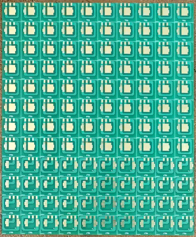
Double Sided PCB Board
| Feature | Advantage | B2B Use Case |
|---|---|---|
| Dual-Layer Routing | Increased component density | Telecom equipment |
| Cost-effective | Cheaper than multilayer | Automation hardware |
| Design flexibility | Easier revisions | Consumer electronics |
Here’s the real story about double-sided PCBs—you can pack lots of circuitry onto a compact board, but only if you understand how materials and design features work together.
A double-sided PCB board consists of two copper-clad layers—top and bottom—separated by a dielectric substrate. To electrically connect both sides, plated through-holes (PTHs) are essential. These allow traces and components to interconnect across layers seamlessly.
Ready for the good part? A medical device supplier we worked with needed a compact control board. They designed top-layer logic and bottom-layer power distribution, connecting both through multiple via clusters. The result: better thermal separation and a 20% cost saving compared to a multilayer alternative.
But it’s not just about placement—you must optimize trace widths, via sizes, and clearance rules. Follow IPC-2221 spacing guidelines and factor in copper weight and current density. For example, a motor driver board requires wider traces (~20 mil) compared to a sensor board (~8 mil). According to IPC-2221, traces should carry ≤10 A without exceeding 10 °C temperature rise when properly designed.
| Parameter | Recommended Value | Notes |
|---|---|---|
| Trace Width | 8–20 mil | Depends on current load |
| Via Diameter | 0.3–0.6 mm | Balance reliability & routing |
| Copper Thickness | 1–2 oz | Standard for double-sided boards |
| Clearance | 6–10 mil | Per IPC-2221 standards |
The benefits of a double sided PCB board go far beyond simply adding another copper layer. But here’s the kicker… companies that adopt double-sided boards often realize tangible savings in cost, space, and performance before they even scale to multilayer designs.
First off, you get increased circuit density. By routing signals on both sides, engineers can halve the board area compared to equivalent single-sided designs. Case in point: a medical imaging startup reduced their control board size from 80 mm × 120 mm to 50 mm × 80 mm, enabling a slimmer device. At the same time, industrial sensor manufacturers achieved 30% fewer via jumps by moving components to the reverse side.
Cost-effectiveness is another story. A B2B electronics supplier moved to double-sided boards instead of multilayer substrates and saw a 25% cost drop per board, without compromising design integrity or performance. That buyer saved enough to invest in custom housings and expand production volume.
Here’s the real story: double-sided boards offer a middle ground—more capability than single-layer but significantly cheaper and easier than multilayer. Plus, sourcing is simpler: most PCB fabricators specialize in volumes and turnaround times for double-sided boards, often offering 2–4 day delivery vs. 7–10 days for multilayer.
Finally, they improve thermal and EMI performance. With power traces on one side and signal traces on the other, heat dissipation improves and crosstalk is reduced. A telecom integrator noticed a 15% decrease in emissions after moving to well-separated layers aligned with proper ground plane strategy.
| Benefit | Double-Sided PCB | Single-Sided PCB | Multilayer PCB |
|---|---|---|---|
| Circuit Density | High | Low | Very High |
| Cost per Unit | Moderate | Low | High |
| Manufacturing Ease | Easy | Very Easy | Moderate |
| Lead Time | 2–4 days | 1–2 days | 5–10 days |
| EMI & Thermal Control | Good | Poor | Excellent |
What’s the real story regarding double sided pcb board adoption? Industries across the board—from consumer gadgets to industrial control—are realizing the strategic advantage of double-sided PCBs.
Consumer electronics is a standout. A wearable tech brand placed user interface components on one side and power regulation on the other, making their compact design both functional and robust. They cut board count in half—boosting margins and reducing assembly labor.
In automotive, ECU manufacturers routinely use double-sided boards for sensor and actuator modules where cost sensitivity meets performance. Just ask a supplier that reduced assembly errors by 40% thanks to simplified placement and standardized drill vias.
LED lighting is another big adopter. A lighting OEM migrated from single-layer boards to double-sided ones, adding thermal pathways on the reverse side to significantly improve heat sinking under high-power LED arrays. That move extended product lifespan by 25% and reduced warranty returns.
Even industrial automation equipment makers leverage this tech. Robotics controller boards use double-sided designs with high-voltage power trace isolation on the bottom and signal routing on top, allowing efficient assembly without resorting to expensive flex multilayer boards.
Here’s why it matters for your B2B purchasing decisions: double-sided PCB boards deliver versatility without drastically increasing cost or supply chain complexity. They’re widely available, quick to fabricate, and well understood by OEMs and EMS providers.
| Industry | Use Case | Benefits |
|---|---|---|
| Consumer Wearables | Power on reverse, sensors on top | Compact design, faster assembly |
| Automotive ECUs | Dual-layer routing for logic/control | Cost-effective, reduced assembly errors |
| LED Lighting | Heat dissipation via copper layers | Extended lifespan, better thermal management |
| Industrial Controls | High-voltage + signal isolation | Reliable design, avoids multilayer costs |
When it comes to choosing materials for your double sided pcb board, the right choice can make or break your product’s reliability and performance. But here’s the kicker… selecting the wrong substrate or copper weight could lead to failures in the field or unnecessary cost inflation.
Let’s break it down with real-world context. A medical instrument OEM switched from standard FR4 to high-TG FR4 and saw a 30 °C improvement in thermal performance during sterilization cycles—critical for medical certification. Another case: a telecommunications firm adopted copper thickness upgrades from 1 oz to 2 oz, enabling them to deliver 5 A power handling capabilities without trace burnouts. And a LED lighting manufacturer chose aluminum-backed substrates for high-power boards, reducing thermal hotspots by 40%.
Substrate type matters:
• FR4 remains the most versatile and cost-effective choice.
• High-TG FR4 enables higher temperature tolerances and thermal shock resistance.
• Polyimide is preferred for flex or rigid-flex designs in aerospace and medical devices.
• Aluminum-backed boards offer superior heat dissipation, ideal for LED or power modules.
Copper thickness options:
• 1 oz (35 µm) – standard electronics
• 2 oz (70 µm) – moderate power applications
• Heavy copper (≥4 oz) – industrial drives and motor controllers
Here’s a handy table to compare your material options:
| Material Type | Typical Use Case | Strengths | Drawbacks |
|---|---|---|---|
| FR4 | General electronics | Affordable, stable | Not for extreme heat or flex |
| High-TG FR4 | Industrial, automotive | Better thermal performance | Slightly more expensive |
| Polyimide | Flex PCBs, aerospace | Flexible, heat-resistant | Costly, specialized handling |
| Aluminum-backed | LED power modules | Excellent heat sinking | Harder to drill, rigid |
| 1 oz Copper | Standard routing | Balanced cost and conductivity | Limited for high-current designs |
| 2 oz Copper | Power circuits | Handles up to ~5 A traces | Slightly higher cost |
| 4–10 oz Copper | Industrial power, motor drives | Supports high current | Needs precise etching, expensive |
What’s the real story? If you’re producing moderate power electronics with thermal demands, high‑TG FR4 paired with 2 oz copper is the sweet spot. If you’re pushing thermal or mechanical limits, polyimide or aluminum-backed boards may be necessary. Planning for future scalability can save costly redesigns later
So you’re ready to design—but where do you start? Here’s the real story… without a structured workflow, even the best double sided pcb board can fail in production. A methodical approach ensures reliability, manufacturability, and performance.
Let’s walk through each stage with business-focused examples:
Schematic Capture
Begin with a clear, validated circuit diagram. Use tools like Altium, KiCad, or Eagle. In one telecom project, engineers used Altium’s integrated library to ensure accurate component footprints and net connectivity before any layout. In another automotive sensor project, KiCad’s ERC (Electrical Rules Check) identified ground-loop risks early, avoiding EMI failures.
PCB Layout and Signal Layer Routing
Place high-speed components (like CPUs or RF modules) first, grouping decoupling capacitors and power regulators closely. A consumer drone startup arranged sensors and power regulators on opposite sides of the board to improve thermal separation—using double sided routing to meet tight weight limits. Designers routed analog and digital grounds on separate plane layers and connected them through a single star-point via to minimize noise.
Design for Manufacturability (DFM)
Follow IPC spacing and trace standards. Use standardized drill sizes and check panel utilization. A B2B industrial control board was rejected by their supplier because the board outline didn’t meet panel breakaway rules. After a quick adjustment, scrap rate dropped 15%. Ensure trace-to-via clearances and minimize blind vias—double sided boards shouldn’t rely on HDI unless necessary.
DRC and Emerging Checks
Run design rule checks for clearance, hole-to-pad ratios, silkscreen overlaps, and minimum trace widths. A medical device OEM found surviving silkscreen overlapping test pads just before sending files—catching it prevented a failed reflow run. Always preview Gerber layers to catch odd misplacements.
| Design Step | Key Considerations | Tools/Actions |
|---|---|---|
| Schematic Capture | Net connectivity, component accuracy | ERC in EDA tools |
| Component Placement | Thermal, mechanical, routing grouping | Floorplan review, placement grid |
| Routing | Trace width, impedance control, via usage | Manual/auto-router + impedance checks |
| DFM Compliance | Panel breaks, drill standards, trace spacing | Supplier DRC or panel checklists |
| Final Verification | Layer alignment, silkscreen masking, Gerber preview | Gerber viewer, 3rd‑party review |
Ready for the good part? With a bulletproof design and DFM alignment, you’re now set for manufacturing—but first, let’s explore the detailed manufacturing steps, starting with drilling, plating, and layering.
But here’s the kicker… the manufacturing of a double sided pcb board involves far more precision than meets the eye. Layer alignment, drill accuracy, plating consistency—they all dictate whether your board ends up functional or flawed.
Drilling & Layer Alignment
Drilled holes must align top-to-bottom within ±10 µm for trace integrity. For example, an automotive sensor board used 0.4 mm vias and required offset control within 7 µm. Laser registration marks and high-precision drills are key.
Through‑Hole Plating
After drilling, through-holes get plated with copper to connect both layers electrically. A defense electronics supplier implemented pulse plating techniques to maintain even thickness across dense drill regions—else test failure rates jumped 20%.
Laminate Pressing (for double sided only)
Double sided boards undergo a lamination cycle to bond copper layers under heat and pressure. This stabilizes trace alignment. A robotics OEM found skipping post-drill cleaning led to delamination in storage—adding a clean + laminate step solved it.
Solder Mask and Silkscreen Application
Liquid Photoimageable (LPI) solder mask protects all but pads. Automated pick-and-place and reflow processes depend on this precision. A packaging machinery manufacturer standardized green solder mask for automated inspection clarity.
Final Surface Finish
Choose HASL, ENIG, or OSP based on application. High-reliability PCBs opt for ENIG despite cost premiums for lead-free finish and excellent pad flatness.
| Stage | Description | Quality Control Metric |
|---|---|---|
| Drilling & Alignment | Precise hole location across layers | ±10 µm offset measurement |
| Through‑Hole Plating | Copper deposition inside holes | 20–25 µm plating thickness |
| Lamination | Heat & pressure bonding for board stability | Adhesion peel & X-ray |
| Solder Mask Application | Insulates and protects copper traces | Mask registration accuracy |
| Surface Finish | Prepares pads for soldering and assembly | Finish type & pad wetting tests |
Ready for the good part?
Testing isn’t just a final step—it’s a strategic assurance that your double sided PCB board will perform reliably in the field. With proper testing, you protect your brand, meet industry standards, and reduce return rates.
Let’s dive into five common testing methods:
Flying Probe Testing
This method uses movable probes to check electrical continuity and shorts across nets. In a small-batch industrial sensor order, flying probe testing found a misrouted trace before assembly—saving thousands in scrap.
In‑Circuit Testing (ICT)
A fixture board checks components like resistors and capacitors post-placement. A medical device OEM used ICT to validate for 100% of production boards with traceable serial numbers, ensuring each unit met specs.
Automated Optical Inspection (AOI)
High-resolution cameras examine solder mask registration, silkscreen clarity, and component orientation. A lighting control board manufacturer cut failure rates by 50% after upgrading AOI.
X‑Ray Inspection
Essential for boards with hidden joints like BGAs or inner-layer vias. A drone navigation PCB, with buried vias, passed FAA certification thanks to full X‑ray sign‑offs.
Functional Testing
End‑use performance tests occur before shipment. A telecom firm’s base-station prototypes underwent live-load simulation prior to approval.
| Test Type | Purpose | Typical Use Case |
|---|---|---|
| Flying Probe | Continuity and shorts | Small batch validation |
| In‑Circuit Test | Component functionality | High-volume production |
| AOI | Visual defects | All surface-mount boards |
| X‑Ray Inspection | Hidden joint integrity | BGAs, multi-layer boards |
| Functional Test | Final performance | System-level validation |
But here’s the real story… testing is your last line of defense against costly recalls. Data-driven quality assurance leads to stronger supplier relationships and greater market confidence.
Next, let’s explore assembly considerations—because once the PCB is proven, components must be mounted reliably.
What’s the real story behind seamless PCB assembly? Precision placement, process alignment, and thermal awareness are critical—especially on a double sided PCB board.
Surface Mount Technology (SMT) first
Components mounted on the top side, followed by reflow soldering. Later, vacuum pick-and-place machines position components, and reflow ovens solder them—creating reliable surface connections.
Through-Hole Components next
Once SMT is complete, through-hole parts—like connectors—are inserted from the top and soldered by wave or selective soldering on the underside. A consumer electronics client improved throughput 20% by staggering SMT and wave steps separately.
Rigid Component Placement
On double-sided boards, identical reflow on both sides isn’t feasible. So placement order matters: mount and reflow major components on one side, cool the board, flip it, then execute the second reflow—carefully managing thermal cycles to avoid solder fatigue.
Heat Management
One industrial control board manufacturer added thermal relief patterns to reduce heat accumulation during reflow. That adjustment increased yield by 15% by avoiding tombstoning of resistors.
| Step | Action | Key Considerations |
|---|---|---|
| SMT Placement | Pick-and-place, plus first reflow | Profile to component spec |
| Through-Hole Insertion | Manual or automated part placement | Precision alignment essential |
| Wave/Selective Solder | Solder underside pads | Avoid thermal shock |
| Cooling & Inspection | Visual & AOI inspection | Look for tombstones, voids |
| Final Test Fit | Functionality and enclosure integration | Confirm connectors and dimensions |
This is where it gets interesting… Choosing between a double sided PCB board and a multilayer design is about balancing complexity, cost, and performance.
Double sided boards support two copper layers bonded across a dielectric, suitable for most mid-complexity products. Multilayer PCBs, by contrast, stack three or more layers into a single board and require advanced lamination, controlled impedance, and complex design techniques. That extra complexity adds cost—often 50–100% more per unit—and lengthens lead times. But the trade-off can be worthwhile for high-speed designs, compact RF modules, or medical implants needing precise layer structures.
Consider three examples: An audio amplifier supplier used multilayer boards to minimize EMI, but only after moving from single to double sided prototypes to validate initial layouts. A telecom OEM chose double sided for low-volume sensor arrays, saving 35% compared to multilayer versions. And a satellite hardware startup used multilayer boards for bundled board designs under tight RF specifications. By comparing cost, density, lead time, and technical risk, they confirmed double sided PCBs offered the best balance for their use case.
| Factor | Double Sided PCB | Multilayer PCB |
|---|---|---|
| Cost per Board | Moderate | High |
| Circuit Complexity | Medium | Very High |
| Lead Time | 2–5 days | 7–14 days |
| EMI Performance | Good (with care) | Excellent |
| Design Difficulty | Low | High |
Choosing the right board depends on technical requirements and cost constraints. Double sided boards hit a sweet spot for many B2B applications: offering high performance without the premium of multilayer manufacturing.
But here’s the kicker… even well-intentioned designs can hit real-world challenges. Let’s unpack the top issues you face and how professionals solve them.
Signal Integrity & Crosstalk
Routing signals on both sides increases risk of electromagnetic coupling if not separated properly. A fiber-optic transceiver embedded-too-close signal lines and power traces, causing cross-talk that manifested only at full speed. Engineers resolved it by adding ground stitch vias and a copper pour plane to direct return currents.
Thermal Management
Double sided boards often carry power and signal layers. If you route power traces on one side and dissipate heat on both, thermal stress builds up. A motor controller board burned traces under load due to narrow traces. Increasing trace width to 25 mil and using heat-sinking vias fixed the issue.
Manufacturing Tolerances
Dual-layer alignment relies on precision drilling and lamination. Misalignments above ±15 µm caused pads to misregister, leading to solder bridging. Working closely with suppliers, one tooling team adjusted drill fixtures and added registration marks to ensure consistent panel alignment.
Component Access & Rework
Dense via placement and component overlap can make rework difficult. One consumer IoT product design clustered connectors too tightly, making late-stage firmware debugging hard. Redesigning for larger via annular rings and adding test points improved serviceability.
| Challenge | Impact | Professional Fix |
|---|---|---|
| Crosstalk & EMI | Signal interference at high frequency | Add ground pours and via stitching |
| Thermal Overload | Trace burnout under current load | Increase width and thermal vias |
| Misalignment | Solder bridging and pad misregistration | Use tighter drill tolerance and pads |
| Rework Difficulty | Hard debugging or repair | Design for test and spaced components |
Mastering these challenges early avoids costly re-spins and quality failures in the field.
What’s the real story behind budget-smart PCB procurement? It’s about smart design, material choice, process alignment—and collaboration—with your manufacturer.
Optimize Panel Usage
Arrange multiple boards per panel using nest-to-fit layout—it reduces edge waste and lowers per-unit cost. One EMS provider charges 20% less when customers submit nested panels.
Standardize Hole Sizes & Specs
Using common drill sizes across your board avoids small drill charges. A robotics OEM reduced tooling fees by 70% by using only 0.6 mm vias.
Use Common Surface Finishes
Default finishes like HASL are cheaper than specialty options like gold ENIG. Many B2B products don’t need ENIG. A telecom supplier only used ENIG for gold-plated edge connectors.
Minimize Layers Where Possible
Avoid unnecessary layers. A smart meter producer saved 40% by using double-sided boards with good routing instead of jumping to 6-layer boards prematurely.
Design for Manufacturer Feedback
Share your requirements early, and leverage your PCB fabricator’s DFM checks. Professionals catch routing violations before board order placement—saving rework later.
| Strategy | Benefit | Example Outcome |
|---|---|---|
| Nesting Panels | Lower fabrication cost per board | 20% production cost savings |
| Standard Drill Sizes | Avoid special tooling charges | 70% cheaper setup costs |
| Default Surface Finishes | Save vs premium finishes | ENIG reserved for critical pads only |
| Layer Minimize | Lower complexity without sacrificing quality | 40% board cost reduction |
| DFM Collaboration | Avoid pre-production errors | Zero revisions on first production panel |
Ready for the good part? Choosing your PCB manufacturer is more than just cost—it’s about capabilities, quality, and partnership.
Start by assessing capability matching. Not all fabs can reliably produce double sided PCB boards with tight tolerances or heavy copper. A defense contractor selected a TI‐certified fab to meet trace impedance specs, while an IoT startup went local for cost and speed. Identify whether you need high-TG materials, 2 oz copper, or ENIG finishes—and ensure your supplier supports it.
Next, check certifications and compliance. Many markets require ISO 9001, IPC-6012, UL certification, or automotive-specific IATF approval. A medical device maker chose a UL-recognized PCB shop to meet regulatory demands and fast-track product certification.
Evaluate lead times and support. A telecom equipment supplier found that partnering with a fab offering 3-day prototyping cycles saved six weeks in their development timeline. That’s why lead time transparency matters. Don’t just get a price quote—ask about real lead time under current load.
Don’t overlook communication and support. A robotics company benefited from a fab providing immediate design-for-manufacturability (DFM) feedback, avoiding costly re-spins. A proactive fab asks questions and flags issues early—that partnership is worth its weight in gold.
| Criteria | Why It Matters | Checkpoint |
|---|---|---|
| Capabilities | Ensures board specs are met | Ask about layers, copper weight, materials |
| Certifications | Meets industry or regulatory standards | ISO, IPC, UL, IATF |
| Lead Time | Impacts project scheduling | Confirm typical turnaround, prototype options |
| Communication Quality | Prevents errors and delays | Check engineer responsiveness, DFM support |
Choosing a fab isn’t just procurement—it’s forming a strategic alliance. The right partner accelerates your roadmap and safeguards quality.
This is where it gets interesting… As electronics evolve, double sided pcb board manufacturing is keeping pace with tech advances and shifting demands.
Miniaturization & HDI Adoption
As devices shrink, High-Density Interconnect techniques—like microvias and laser-drilled through-holes—are increasingly employed even on double sided boards. A wearable manufacturer now uses 0.1 mm vias to pack more features into wrist-size architectures.
Eco-Friendly Materials
Roadmaps toward sustainability are shaping material selection. Water-soluble solder masks and formaldehyde-free laminates are gaining traction. One appliance OEM reported a 20% reduction in waste and streamlined disposal through greener materials.
Embedded Components
Embedding passive components—like resistors or capacitors—into the substrate makes double sided boards more powerful. A telecom board integrated chip resistors within its core layer, reducing assembly time by 30%.
Smart Manufacturing & IoT‑Connected Fabs
Manufacturers are adopting IoT sensors to monitor pressure, temperature, and humidity in real time, ensuring precision every step. High-precision fabs now generate Machine Data Systems (MDS) reports to flag process drift before it affects quality.
| Trend | Description | Impact |
|---|---|---|
| HDI Techniques | Use of microvias, finer traces | Higher density without multilayer cost |
| Sustainable Materials | Eco-friendly laminates and masks | Lower waste, regulatory compliance |
| Component Embedding | Passive components built into layers | Faster assembly, compact designs |
| IoT‑Connected Fabrication | Real-time sensor monitoring in manufacturing | Improved yield, predictive maintenance |
Staying aware of these trends helps you future-proof your PCBs—making smart investment decisions today.
Conclusion
So what’s the real story behind mastering double sided pcb boards? It’s all about understanding materials, design precision, manufacturing workflows, and strategic supplier selection. You’ve seen how double-sided boards deliver a sweet spot of performance, cost efficiency, and manufacturability for many B2B applications.
Remember: optimally designed double-sided boards can slash size, support complex electronics, and meet regulatory demands without requiring the expense of multilayer production. Pair that with smart cost-saving strategies and a strong manufacturing partner—and you’ve got a product that stands out in reliability, speed-to-market, and total cost of ownership.
Make these insights your baseline. Whether you’re launching a new product or optimizing supply chains, double sided pcb boards offer a powerful toolkit. Now get out there and build something exceptional.
FAQ Section
Q1: What is a double sided PCB board?
A double sided PCB board has conductive copper on both its top and bottom surfaces, connected through plated through-holes, enabling greater circuit density and flexibility over single-sided boards.
Q2: How does a double sided PCB work?
It routes signals on both faces of the board and uses plated through-hole vias to connect layers, allowing compact, efficient component placement and trace distribution.
Q3: What are the advantages of using double sided PCBs?
They offer improved circuit density, better thermal and EMI performance, shorter lead times, and cost savings compared to multilayer boards.
Q4: Can I use surface mount and through-hole components on both sides?
Yes, as long as reflow and wave soldering profiles are carefully managed, components can be placed on both sides with proper sequencing and thermal control.
Q5: How do I choose the best material for my double sided PCB?
Select based on application needs—standard FR4 for general use, high-TG FR4 for temperature resilience, polyimide for flex, or aluminum-backed for heat-heavy designs.


Connect to a Jerico Multilayer PCB engineer to support your project!
Request A Quote


 Quote
Quote