


+86 13603063656
When it comes to high-performance printed circuit boards (PCBs), ENIG PCBs are one of the most popular choices. But here’s the kicker? ENIG, which stands for Electroless Nickel Immersion Gold, is a surface finish that offers multiple benefits for various electronic applications. This blog post dives into what ENIG PCBs are, how the process works, their advantages, and where they are most commonly used. By the end of this article, you’ll have a solid understanding of why ENIG PCBs are a top choice for manufacturers worldwide.
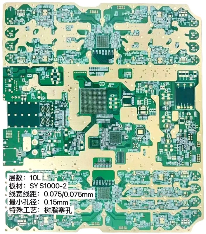
ENIG PCB
To understand ENIG PCBs, we first need to know what ENIG stands for. ENIG stands for Electroless Nickel Immersion Gold. But what’s the real story? ENIG is a surface finish technique used in PCB manufacturing where a layer of electroless nickel is applied to the PCB surface, followed by an immersion gold layer. This finish is essential for enhancing the quality of the PCB, particularly in ensuring reliable solder joints and durability.
The electroless nickel provides corrosion resistance, while the gold offers excellent solderability and helps protect the nickel layer. This combination makes ENIG an excellent choice for PCBs that will undergo high-performance applications, such as those found in consumer electronics, automotive, and medical devices.
ENIG is often preferred over other finishes because it provides a smooth, even surface that is ideal for fine-pitch components, which are common in modern electronic devices.
Table 1: What is ENIG?
| Term | Description |
|---|---|
| Electroless Nickel | A nickel layer deposited onto the PCB surface without the use of electricity |
| Immersion Gold | A thin gold layer applied to the nickel for better solderability and protection against corrosion |
The process of creating an ENIG PCB involves several key steps, each of which is crucial for achieving the desired quality and performance. Ready for the good part? Here’s a step-by-step breakdown of how the ENIG process works.
Before applying the electroless nickel, the PCB is cleaned to ensure that no contaminants are present on the surface. This cleaning process involves using chemicals to remove oxidation, oils, and dirt. This step is vital for ensuring that the nickel will bond properly with the copper layer of the PCB.
Next, the PCB is submerged in a chemical bath where the electroless nickel is deposited onto the surface. This process does not require an electrical current, as the nickel is chemically plated onto the PCB. The result is a layer of nickel that provides corrosion resistance and mechanical strength.
After the nickel has been deposited, the PCB is immersed in a gold solution. The immersion gold is then plated over the nickel layer. This gold layer serves as an excellent barrier to prevent oxidation and provides superior solderability. The thickness of the gold layer is usually around 0.05 to 0.1 microns.
Once the ENIG process is complete, the PCB is subjected to rigorous testing and inspection to ensure the finish meets quality standards. This includes checking for any defects or irregularities in the gold and nickel layers, as well as ensuring that the surface is smooth and free of contamination.
Table 2: ENIG Process Overview
| Step | Description | Purpose |
|---|---|---|
| Pre-Treatment | Cleaning the PCB surface | Ensures proper bonding of nickel |
| Electroless Nickel | Nickel plating applied to the PCB surface | Provides corrosion resistance and strength |
| Immersion Gold | Gold layer applied over the nickel | Improves solderability and protects against oxidation |
| Final Inspection | Visual and functional checks | Ensures finish meets quality standards |
Why is ENIG PCB finish so widely used? Let’s break it down. Ready for the kicker? The advantages of ENIG PCBs are numerous, making them an excellent choice for a wide variety of applications. Here are some of the key benefits of using ENIG for PCB surface finishes:
The nickel layer provides an excellent barrier against oxidation, ensuring that the PCB stays functional even in harsh environments. The gold layer adds an additional level of protection, especially when exposed to moisture and air, which can cause other finishes to degrade.
ENIG finishes are highly solderable due to the smoothness of the gold layer. This is especially important for fine-pitch components, where precision is crucial. ENIG ensures that components can be soldered easily, reducing the risk of defects during assembly.
ENIG PCBs provide a highly flat surface. This is crucial for ensuring that components, especially surface-mount devices (SMDs), sit correctly on the board. The uniformity of the surface improves the reliability of the solder joints and reduces the risk of component misalignment.
ENIG is particularly beneficial for PCBs that require fine-pitch components, such as BGAs (Ball Grid Arrays), due to its smooth and even finish. Fine-pitch components require precision soldering, and ENIG provides the perfect surface for this.
Table 3: Benefits of ENIG PCB Finish
| Benefit | Description | Importance |
|---|---|---|
| Corrosion Resistance | Gold and nickel layers protect against oxidation | Improves durability |
| Superior Solderability | Smooth finish ensures easy and reliable soldering | Reduces assembly defects |
| Flatness | Even surface for proper component placement | Essential for precise soldering |
| Fine-Pitch Compatibility | Ideal for components like BGAs | Enables efficient high-density designs |
ENIG is often compared to other surface finishes like HASL (Hot Air Solder Leveling), OSP (Organic Solderability Preservative), and Immersion Silver. But here’s the kicker? While each finish has its own set of advantages, ENIG stands out for its solderability and reliability in high-performance applications.
HASL is one of the most commonly used PCB finishes, but it has some limitations compared to ENIG. HASL involves dipping the PCB into molten solder, which can result in uneven thickness and potentially less reliable solder joints. ENIG, on the other hand, offers a smooth and consistent surface that is ideal for fine-pitch components and ensures better long-term performance.
OSP is an organic finish that provides good solderability but is less durable compared to ENIG. OSP is ideal for single-layer PCBs, but ENIG is preferred for more complex designs, especially those that require better reliability and longer shelf life.
Immersion Silver offers similar performance to ENIG in terms of solderability, but it is less durable and prone to tarnishing over time. ENIG’s gold layer offers superior protection and long-term reliability, especially in high-humidity environments.
Table 4: ENIG vs. Other Surface Finishes
| Finish | Advantages | Disadvantages |
|---|---|---|
| ENIG | Superior solderability, durability, ideal for fine-pitch components | Higher cost compared to some alternatives |
| HASL | Inexpensive, widely used | Uneven thickness, less reliable for fine-pitch |
| OSP | Environmentally friendly, good solderability | Less durable, not ideal for multi-layer PCBs |
| Immersion Silver | Good solderability, cost-effective | Tarnishes over time, less durable than ENIG |
ENIG PCBs are commonly used in a wide range of industries, particularly in devices that require high performance and durability. Ready for the good part? Here’s where ENIG really shines.
ENIG finishes are widely used in smartphones, laptops, and other consumer electronics. These devices require high-density circuits and fine-pitch components, making ENIG an ideal choice for ensuring reliability and performance.
ENIG PCBs are also used in the automotive industry for applications such as engine control units (ECUs) and safety systems. These systems must withstand harsh environmental conditions, and ENIG’s durability and corrosion resistance make it perfect for these applications.
In medical devices, where reliability is crucial, ENIG PCBs ensure that the connections between components remain stable and durable. ENIG is used in life-saving devices like pacemakers, defibrillators, and monitoring systems, where quality and performance cannot be compromised.
Table 5: ENIG PCB Applications
| Industry | Application | Example Devices |
|---|---|---|
| Consumer Electronics | Smartphones, laptops, tablets | iPhone, MacBook |
| Automotive | Engine control units, safety systems | Airbag systems, anti-lock braking |
| Medical | Life-saving devices, diagnostic equipment | Pacemakers, heart monitors |
In conclusion, ENIG is a highly versatile and reliable PCB surface finish that provides numerous benefits, including excellent solderability, corrosion resistance, and compatibility with fine-pitch components. Ready for the kicker? If you’re looking for a finish that offers superior durability, smoothness, and long-term reliability, ENIG is the go-to choice. Whether you’re designing PCBs for consumer electronics, automotive applications, or medical devices, ENIG is a trusted finish that meets the demands of high-performance circuits.
FAQ Section
Q1: What is ENIG in PCB?
A1: ENIG (Electroless Nickel Immersion Gold) is a surface finish used in PCB manufacturing that involves depositing a nickel layer followed by a gold layer to enhance solderability, corrosion resistance, and flatness.
Q2: How is ENIG different from HASL?
A2: ENIG offers a smoother surface, better durability, and is ideal for fine-pitch components, while HASL can have uneven thickness and is less reliable for high-density designs.
Q3: What are the benefits of using ENIG for PCBs?
A3: ENIG provides excellent corrosion resistance, superior solderability, a smooth surface for component placement, and better reliability, especially for fine-pitch components.
Q4: Can ENIG be used in automotive and medical devices?
A4: Yes, ENIG is ideal for use in automotive and medical devices, as it offers high durability, corrosion resistance, and reliability, which are essential in these industries.
Q5: Is ENIG expensive compared to other finishes?
A5: Yes, ENIG is generally more expensive than finishes like HASL, but its durability, reliability, and superior performance make it worth the investment for high-performance applications.


Connect to a Jerico Multilayer PCB engineer to support your project!
Request A Quote


 Quote
Quote