


+86 13603063656
Ball Grid Array (BGA) PCBs are the unsung heroes of compact, high-speed electronics. As devices continue to shrink in size but grow in performance, the role of BGA PCB design has become more vital than ever. In this comprehensive guide, we’ll explore everything from the nuts and bolts of BGA packaging to advanced manufacturing processes, inspection techniques, and industry applications. Whether you’re a seasoned engineer or sourcing expert looking to optimize your supply chain, this article is tailored to offer insights, practical takeaways, and the clarity you need to work confidently with BGA PCB technology.
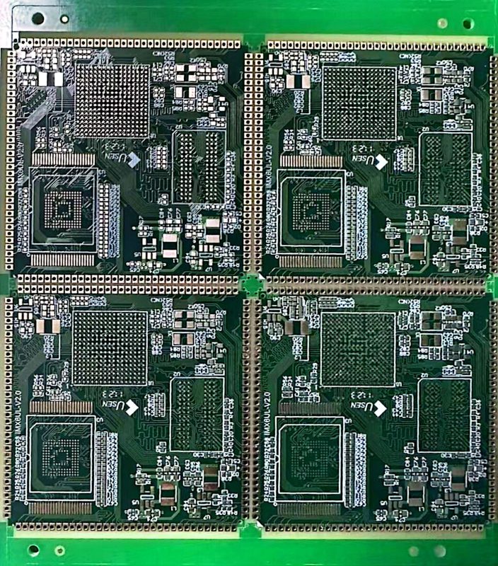
High-Precision BGA PCB
Let’s start with the basics—what exactly is a BGA PCB? A BGA (Ball Grid Array) PCB is a printed circuit board that uses a grid of solder balls to mount integrated circuit (IC) packages. These balls sit beneath the component and provide both the electrical connection and mechanical stability. BGA technology emerged as a solution to the limitations of older packaging methods like QFP (Quad Flat Package), especially in high-pin-count and high-performance applications.
But here’s the kicker… BGA PCBs don’t just reduce size—they improve reliability, thermal performance, and signal integrity. The evolution from traditional pin-through-hole packages to surface-mount technology and eventually to BGA opened new doors for miniaturization and high-speed performance.
Modern devices like smartphones, GPUs, and routers are impossible without BGA PCBs. These boards allow manufacturers to pack more processing power into smaller spaces, enabling everything from advanced gaming to AI computations. And as AI, 5G, and IoT continue to grow, so does the demand for reliable and high-density BGA PCB solutions.
The world of BGA is vast, but let’s break it down. At its core, BGA is a type of surface-mount packaging where the connection points—the solder balls—are arranged in a grid on the bottom of the component. During assembly, these balls melt and bond with the PCB pads, forming strong electrical and mechanical connections.
What’s the real story? It’s not just one type of BGA. There are several variations:
Each type serves different use cases depending on thermal needs, durability, and environmental exposure. For example, CBGA offers excellent thermal dissipation and is used in automotive or military applications. PBGA is cost-effective and perfect for consumer electronics.
So why choose BGA? Simply put—better electrical performance. The short connections reduce inductance, and the grid layout ensures even current distribution. Add in excellent thermal management and more robust mechanical structure, and you’ve got a packaging solution that’s hard to beat.
BGA PCBs are more than just tiny solder balls. Let’s dive deeper.
First, you have the substrate material, typically FR4 or high-Tg laminate, which acts as the backbone. Then, the solder balls, made primarily of tin-lead or lead-free alloys, are pre-deposited on the chip’s underside. When reflowed, they provide electrical pathways and hold the component in place.
Ready for the good part? There’s also underfill—a crucial material injected under the BGA after soldering. This epoxy-based filler adds mechanical strength, improves thermal cycling reliability, and reduces the risk of solder joint cracks. Without it, repeated heating and cooling can destroy your PCB.
| Component | Material Used | Function |
|---|---|---|
| Substrate | FR4, Polyimide | Base support for the PCB |
| Solder Balls | Tin-lead, SAC305 | Electrical & mechanical connection |
| Underfill | Epoxy resin | Thermal stress relief |
| Pads/Vias | Copper with ENIG | Routing for signal and power |
BGA PCBs succeed not just because of clever packaging, but because each component works in harmony to deliver high performance, especially in rugged or thermally demanding applications.
BGA PCB design is a balancing act of space, performance, and manufacturability.
Escape routing is where things get tricky. Since BGA pads are under the component, traditional routing doesn’t work. Designers must use fan-out strategies—usually involving vias-in-pad or dog-bone layouts—to connect each ball to a trace or inner layer.
But here’s the kicker… your design must adhere to strict rules:
Fail to follow these, and you’re risking signal integrity or manufacturability issues.
| Design Element | Recommended Value | Note |
|---|---|---|
| Ball Pitch | 0.5 mm to 1.0 mm | Denser pitch = higher complexity |
| Pad Diameter | 0.3 mm to 0.5 mm | Matches solder ball size |
| Via Type | Microvia, Blind, Buried | Based on pitch and layer count |
| Fan-Out Pattern | Dog-bone or via-in-pad | Varies with pitch constraints |
Proper layout upfront saves enormous time, cost, and headaches during fabrication and assembly.
HDI technology and BGA are a match made in electronics heaven.
This is where it gets interesting… As BGA packages shrink, the routing space underneath also tightens. HDI solves this by using microvias, blind vias, and buried vias to efficiently route signals through multiple layers without eating up surface space.
The benefits are massive:
HDI is indispensable when working with BGA pitches below 0.5 mm. It allows for advanced layer stacking like 1-2-1 or 2-4-2, optimizing space and signal flow.
| BGA Pitch | Recommended HDI Stackup | Via Type Used |
|---|---|---|
| 1.0 mm | 4 Layer Standard | Through-hole |
| 0.8 mm | 6 Layer HDI | Blind + Through-hole |
| 0.5 mm | 8 Layer HDI | Microvia + Buried |
| <0.4 mm | 10+ Layer Advanced HDI | Sequential buildup |
HDI enables today’s most powerful electronics—from smartphones to AI accelerators—to operate at blazing speeds without signal degradation.
Stack-up design determines your PCB’s soul. For BGA, it’s everything.
What’s the real story? If you botch your stack-up, you risk EMI issues, poor impedance control, and thermal disasters. An optimized BGA PCB stack-up balances signal layers, ground/power planes, and dielectric spacing for electrical and thermal performance.
Commonly used configurations include:
You’ll also need to ensure controlled impedance for high-speed lines, especially in BGA designs where differential pairs are common.
| Layer Count | Suitable BGA Pitch | Best Use Case |
|---|---|---|
| 4-Layer | 1.0 mm and above | Basic applications |
| 6-Layer | 0.8 mm | Moderate I/O and speed |
| 8-Layer | 0.5 mm | High-speed consumer devices |
| 10+ Layer | <0.5 mm | Servers, AI, aerospace |
Don’t just copy a standard stack-up—design with intent based on your signal, power, and thermal needs.
BGA components run hot, and managing that heat is critical.
Ready for the good part? You have several tricks up your sleeve:
Simulations using tools like ANSYS or SolidWorks Thermal allow engineers to predict hotspots and fix them before production.
Neglecting thermal considerations can cause solder joint fatigue, underfill cracking, or worse—total board failure.
| Technique | Application | Thermal Impact |
|---|---|---|
| Thermal Vias | High-current BGA areas | Moderate |
| Heatsinks | External component cooling | High |
| Copper Planes | Under BGA pads | Medium |
| Underfill Epoxy | Reinforcement, heat spread | High (when used well) |
Thermal design is where good BGA PCBs become great. It’s the difference between “works” and “works reliably for years.”
You can design the perfect BGA PCB—but can you assemble it properly?
The process begins with stencil printing solder paste onto the pads, followed by precision placement using pick-and-place machines. Then, the board enters a reflow oven where solder balls melt and form secure joints.
But here’s the kicker… Without proper reflow profiles and alignment, you risk cold joints or tombstoning. BGA assembly also uses underfill to protect against vibration and temperature cycling.
Rework is possible—but tough. Tools like infrared rework stations and X-ray alignment systems are mandatory.
| Step | Tool Used | Potential Defect |
|---|---|---|
| Solder Paste | Laser Stencil Printer | Misprint, bridging |
| Component Place | Pick & Place Machine | Misalignment |
| Reflow | Reflow Oven | Cold joints, voids |
| Inspection | X-ray / AOI | Hidden cracks, missing balls |
You need experience, precision tools, and quality control to ensure your BGA PCB survives the real world.
If you can’t see it—how do you inspect it?
Automated Optical Inspection (AOI) isn’t enough for BGA. You need X-ray inspection, which can penetrate the package to examine the solder joints. It reveals voids, bridges, and misalignments under the BGA.
For functional testing, ICT (In-Circuit Testing) and Boundary Scan/JTAG are used, especially for large assemblies or high-reliability industries like automotive and medical.
This is where it gets interesting… Functional Test Fixtures (FTFs) simulate real-world use and catch failures that static tests miss.
| Testing Method | Purpose | Equipment Needed |
|---|---|---|
| X-ray Inspection | Check hidden solder joints | 2D/3D X-ray system |
| AOI | Surface defects | High-res camera system |
| ICT | Electrical continuity | Flying probe tester |
| JTAG | Digital logic testing | Boundary scan tool |
Inspection is not optional—it’s your insurance policy for quality and reliability.
Let’s face it—BGA PCB manufacturing isn’t for the faint of heart.
Manufacturers face several challenges, from alignment accuracy during placement to thermal warping during reflow. One of the most notorious issues is solder joint reliability. Since the joints are hidden underneath, any defect can go unnoticed until the product fails in the field.
But here’s the real kicker… Even something as minor as PCB moisture absorption can cause “popcorning” during reflow, where trapped moisture expands and damages the component. Warpage of the board or component can also lead to open circuits or bridging.
Residues from solder flux can create long-term corrosion if not cleaned thoroughly. This is especially important in aerospace or medical applications, where long-term reliability is non-negotiable.
Manufacturers use baking procedures, strict humidity controls, and advanced solder paste formulations to overcome these issues. And of course, choosing the right underfill and using advanced X-ray inspection tools are crucial for long-term durability.
| Issue | Root Cause | Solution |
|---|---|---|
| Solder Joint Cracks | Thermal cycling, poor reflow | Proper reflow profile, underfill |
| Voiding | Excess flux, insufficient paste | Adjust paste amount, reflow temp |
| Misalignment | Poor pick & place calibration | High-accuracy equipment |
| Moisture Damage | Improper storage | Bake components before assembly |
Tackle these proactively, and your yield and reliability rates will soar.
You can design a masterpiece—but if it’s not manufacturable, it’s useless.
Design for Manufacturability (DFM) ensures your design flows smoothly through fabrication, assembly, and testing. For BGA, this means choosing standard pad sizes, ensuring adequate trace clearance, and providing clear layer stack-up documentation.
But this is where it gets interesting… collaborating with your PCB manufacturer early can reveal optimizations you might not even think of. For example, switching from via-in-pad to dog-bone escape routing could simplify manufacturing and cut costs.
Don’t forget about panelization, stencil design, and fiducial marks—all small things that make a big impact on yield.
| Design Area | DFM Tip | Why It Matters |
|---|---|---|
| Pad Design | Follow IPC-7351 standards | Avoids soldering defects |
| Via Placement | Avoid vias-in-pad if possible | Simplifies assembly |
| Trace Clearance | Maintain 5 mil or more | Prevents shorts during fabrication |
| Documentation | Include full stack-up and Gerbers | Reduces manufacturer errors |
The earlier you apply DFM, the smoother—and cheaper—your production run will be.
BGA PCBs power the devices we rely on every day—and those that protect lives.
In consumer electronics, BGA packages are used in smartphones, laptops, and game consoles to reduce form factor while maintaining high processing power. The iPhone’s A-series processors, for example, use advanced BGA packaging for power and heat efficiency.
In automotive electronics, BGAs are found in ADAS systems, engine control units, and in-vehicle infotainment systems. These require not only high-speed operation but also extreme reliability in fluctuating temperature environments.
Medical applications use BGAs in implantable devices, portable diagnostic tools, and wearable monitors due to their small footprint and low power needs.
And here’s where it gets even more critical—aerospace and military applications use ceramic BGAs for their superior thermal and environmental resistance, including in satellites and radar systems.
| Industry | Application Examples | Key BGA Benefit |
|---|---|---|
| Consumer Electronics | Phones, laptops, TVs | High I/O in small package |
| Automotive | Sensors, ECUs, infotainment | Thermal and vibration stability |
| Medical | Monitors, implants | Miniaturization and reliability |
| Aerospace/Military | Guidance systems, satellites | Extreme thermal tolerance |
From entertainment to life-saving equipment, BGA PCBs are the invisible engine making it all possible.
Not all PCB manufacturers are created equal—especially when it comes to BGA.
Start with experience. A reliable BGA PCB manufacturer should have at least 5 years of BGA-specific fabrication and assembly history. Ask for case studies, yield rates, and defect return data to verify performance.
Certifications matter. Look for ISO 9001, IATF 16949 (automotive), ISO 13485 (medical), or AS9100 (aerospace). These validate their ability to handle high-reliability BGA production.
Ready for the good part? Evaluate their equipment list. Do they have 3D X-ray? Can they handle 0.4 mm pitch BGA? Are they using modern AOI and reflow ovens with accurate profiling?
Last but not least—communication. Choose a partner that’s responsive, transparent, and willing to collaborate with your engineering team.
| Evaluation Area | What to Look For |
|---|---|
| Experience | 5+ years with BGA builds |
| Equipment | X-ray, AOI, reflow oven, microvia drills |
| Certifications | ISO9001, IATF16949, ISO13485, AS9100 |
| Communication | Engineering support and design feedback |
| Prototyping Capability | Fast turnaround with consistent quality |
A great manufacturer isn’t just a vendor—they’re your silent engineering partner.
BGA PCBs can get expensive—but knowing where the costs lie helps you optimize.
The most significant cost drivers are layer count, BGA pitch, and via structure. A 0.4 mm pitch BGA with HDI and microvias can cost 3x more than a standard 1.0 mm BGA on a 4-layer board.
But here’s the kicker… choosing the wrong manufacturer or pushing an unoptimized design into production will multiply your cost and time. DFM reviews, early prototyping, and standardizing materials can drastically reduce costs.
Volume matters too. A 1-piece prototype may cost $150, but at 1,000 units, the price drops to less than $5 per board. Don’t forget tooling costs, especially for stencils and test fixtures.
| Factor | Cost Impact | Notes |
|---|---|---|
| BGA Pitch | High (smaller pitch = $) | Requires HDI/microvias |
| Layer Count | Moderate to High | More layers = more labor and material |
| Prototype vs Volume | High | Economies of scale |
| Material Type | Medium | High-Tg and lead-free cost more |
| Testing/Inspection | Medium to High | X-ray and JTAG increase costs |
Smart design + smart sourcing = optimized BGA PCB costs without quality compromise.
BGA isn’t standing still. The future is even smaller, smarter, and more powerful.
Miniaturization continues. Ultra-fine pitch BGA packages (<0.3 mm) are becoming mainstream, especially for AI chips and wearable tech. These require advanced HDI with sequential buildup and laser-drilled microvias.
Integration is the name of the game. System-in-Package (SiP) and 3D ICs are incorporating multiple BGAs into a single module to save space and boost performance.
And here’s the big one… AI, IoT, and 5G are pushing BGA tech to handle faster signal speeds, tighter impedance control, and improved EMI shielding.
Expect improvements in materials, assembly techniques, and thermal management that allow for even denser BGA packages without sacrificing reliability.
| Trend | Description | Application |
|---|---|---|
| Ultra-Fine Pitch BGAs | <0.3 mm pitch | AI chips, mobile SoCs |
| 3D ICs & SiPs | Multiple chips in one package | Servers, GPUs, portable devices |
| Embedded Components | Passive/active inside PCB | Space-saving, RF shielding |
| AI & 5G Requirements | Higher frequencies, better EMI | Telecom, edge computing |
The BGA revolution is far from over—and your designs must keep pace.
BGA PCBs have transformed the electronics landscape by offering compact size, high reliability, and performance at scale. From understanding packaging types and layout challenges to mastering assembly, inspection, and cost control, this guide has walked you through every major aspect of BGA PCB technology. Whether you’re designing for a medical device or sourcing a telecom-grade board, the secret lies in precision, collaboration, and forward-thinking design.
Make your next BGA project your best yet—by partnering with the right team and arming yourself with the knowledge you’ve just gained.
Q1: What is a BGA PCB?
A BGA PCB is a printed circuit board that uses a Ball Grid Array package to mount integrated circuits, allowing for high density and excellent electrical performance.
Q2: How does a BGA package work?
BGA packages use small solder balls arranged in a grid beneath the chip to create electrical connections with the PCB.
Q3: Why is X-ray inspection important for BGA?
X-rays allow inspection of solder joints hidden beneath the package, ensuring quality and functionality.
Q4: What’s the difference between BGA and QFP?
BGA has solder balls under the package while QFP uses visible leads on the sides; BGA supports higher pin counts and thermal performance.
Q5: Can BGA components be reworked?
Yes, but it requires special equipment and expertise such as reballing and precise temperature control to avoid damage.


Connect to a Jerico Multilayer PCB engineer to support your project!
Request A Quote


 Quote
Quote