


+86 13603063656
In today’s fast-paced world of electronics, LED PCB boards have become a core component of efficient and intelligent lighting systems. From smartphones and automotive headlights to medical devices and industrial lighting panels, these compact, high-efficiency boards play a crucial role. But here’s the kicker… understanding LED PCB boards is not just about knowing what they do—it’s about leveraging their performance, thermal efficiency, and cost-saving advantages in real-world B2B applications. This comprehensive guide will walk you through how LED PCB boards work, what they’re made of, how they’re used, and how to choose and design them effectively.
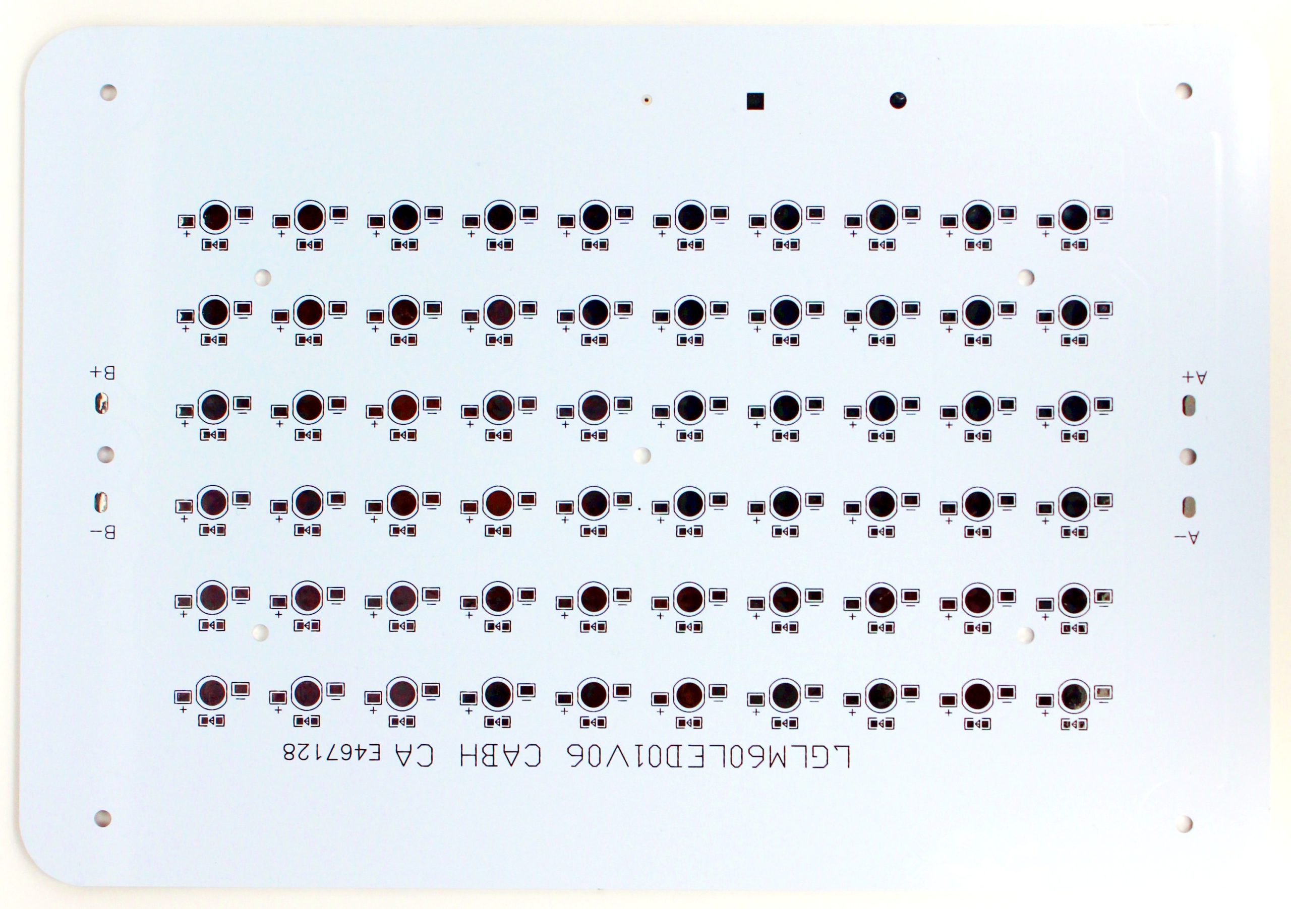
LED PCB Board
LED PCB boards—also known as LED printed circuit boards—are specially engineered to power and support light-emitting diodes (LEDs). These boards not only provide mechanical support but also ensure efficient electrical connectivity and heat dissipation.
What’s the real story? Traditional PCBs struggle with heat. LEDs generate significant heat, and without proper thermal management, the board can fail prematurely. This is where LED PCBs shine—they’re designed with high thermal conductivity materials like aluminum or copper to effectively manage heat.
LED PCBs are vital in a range of sectors. For example, in automotive, they’re used for daytime running lights and dashboard indicators. In industrial automation, they enable reliable machine vision lighting. And in consumer tech? Think smart bulbs, LED TVs, and laptop displays. Their versatility is unmatched.
| Industry | Common LED PCB Applications |
|---|---|
| Consumer | Smart lighting, TVs, laptops |
| Automotive | Headlights, signal lamps, interiors |
| Medical | Surgical lights, scanners, monitors |
| Industrial | Factory floor lighting, sensors |
| Telecommunications | Network devices, control panels |
An LED PCB board works by directing current from the power source to the LED chips through conductive copper traces embedded in the board’s layers. These traces are etched on a thermally efficient base—most often aluminum—to maintain functionality and safety.
But this is where it gets interesting… LEDs produce light through electroluminescence, a process that generates heat as a byproduct. Unlike traditional lighting, this heat must be quickly dispersed to avoid reduced lifespan or color distortion. The LED PCB’s role isn’t just about routing current—it’s about thermally balancing the whole system.
Inside each LED PCB, you’ll find multiple layers working together: conductive copper for signal flow, dielectric insulation for electrical separation, and a metal base for heat conduction. In some designs, thermal vias connect heat sources to external sinks or chassis for extra cooling.
| Layer | Function |
|---|---|
| Copper Layer | Conducts current to LED components |
| Dielectric Layer | Electrically insulates, dissipates heat |
| Base Layer | Provides structural and thermal support |
An LED PCB board might look simple, but beneath the surface, it contains several engineered elements optimized for durability and light quality. So, what exactly goes into one?
Let’s start with the LED chip. This is the light-producing component. It’s mounted on copper pads and bonded with solder. Then we have the driver circuit, responsible for regulating current and preventing burnout. In high-power applications, drivers may be external to the PCB.
But wait—don’t forget the thermal interface material (TIM). Positioned between the LED and the metal core, it improves heat conduction. The solder mask—typically white or black for LED boards—protects copper traces while aiding light reflection or absorption.
Additional features may include lenses or diffusers integrated into the assembly, especially for consumer-facing designs where light dispersion is critical.
| Component | Description |
|---|---|
| LED Chip | Emits light when powered |
| Driver Circuit | Regulates voltage/current flow |
| TIM | Enhances thermal contact with metal core |
| Solder Mask | Protects traces and reflects or absorbs light |
| Heatsink Mounting | Improves thermal dissipation |
Ready for the good part? LED PCB boards come in several types, each tailored to specific use cases. Understanding the differences will help you choose the right solution for your project.
First up is the aluminum LED PCB, by far the most popular. It’s used for applications requiring excellent heat dissipation at an affordable cost—think LED bulbs or automotive lights.
Then there’s the ceramic LED PCB, which uses alumina or aluminum nitride substrates. These offer the highest thermal conductivity and are perfect for high-reliability applications like medical or aerospace lighting.
Flexible LED PCBs use polyimide substrates, allowing them to bend, fold, or twist. They’re used in wearables, interior lighting, and curved screens. Meanwhile, multilayer LED PCBs support high-power LED clusters with separate ground and signal layers to reduce EMI.
| PCB Type | Key Benefits | Typical Application |
|---|---|---|
| Aluminum | Good thermal control, cost-effective | Automotive, general lighting |
| Ceramic | Superior heat transfer, high durability | Medical, aerospace |
| Flexible | Lightweight, bendable | Wearables, displays |
| Multilayer | Supports complex circuits, high power | Stadium lighting, industry |
So why are LED PCB boards taking over the lighting world? Their advantages go far beyond just being compact. These boards provide long-term reliability, energy savings, and design flexibility.
First off, thermal management is unmatched. Aluminum-backed PCBs can lower LED junction temperatures by up to 20°C compared to traditional FR4 boards, greatly increasing lifespan. Secondly, energy efficiency is baked in. Lower resistance means less power loss during operation.
But here’s the kicker… LED PCBs are lightweight, vibration-resistant, and support compact assembly. This makes them ideal for products that require space savings and rugged performance—think drones, bikes, and automotive dashboards.
The cherry on top? They reduce maintenance. With proper design, LED PCB systems can run for 25,000 to 50,000 hours without failure.
| Benefit | Advantage |
|---|---|
| Excellent Thermal Control | Reduces LED burnout and extends lifespan |
| Compact Size | Enables slim, modern product designs |
| High Efficiency | Minimizes power loss |
| Durability | Shock, vibration, and heat resistant |
| Long Operating Life | Up to 50,000 hours of lighting performance |
LED PCB boards are everywhere—and not just in lighting fixtures. Their high efficiency, small footprint, and thermal stability make them a staple in countless industries. But here’s the real story… the application possibilities go far beyond what most expect.
In consumer electronics, LED PCBs illuminate backlit screens in smartphones, tablets, and TVs. For automotive, they power headlights, brake lights, and dashboard illumination—offering energy savings and design flexibility. In the medical field, surgical lamps and diagnostic imaging systems rely on LED PCBs to deliver consistent brightness and color accuracy.
And let’s not forget industrial uses. High-bay lighting in warehouses, machine vision systems, and even robotic arms use LED PCBs for both function and safety. The list goes on into smart cities, IoT street lighting, aerospace panels, and retail displays.
| Application Area | Common LED PCB Uses |
|---|---|
| Consumer | TVs, smartphones, laptops, flashlights |
| Automotive | Headlights, signal lights, dashboard displays |
| Medical | Surgical lights, phototherapy, diagnostics |
| Industrial | Warehouse lighting, machine vision |
| Smart Systems | Streetlights, smart signage, traffic control |
Now let’s get technical—because material choice can make or break your LED PCB’s performance. LED boards are designed to handle high temperatures and require materials that conduct heat efficiently without sacrificing electrical insulation.
Aluminum is by far the most commonly used base material. It’s cost-effective and provides excellent thermal conductivity, which is crucial for high-power LEDs. But what’s the real story? When performance trumps cost, ceramic substrates like alumina and aluminum nitride step in. They offer even better heat dissipation and stability at elevated temperatures.
Above the base lies the dielectric layer, which insulates while allowing heat flow. Dielectric quality directly impacts the board’s thermal resistance. Then comes the copper layer, which provides electrical connectivity. The thickness of this layer (usually 1–2 oz/ft²) also affects thermal and current capacity.
| Material | Function | Thermal Conductivity |
|---|---|---|
| Aluminum | Base layer and heatsink | 1.0–2.0 W/m·K |
| Alumina Ceramic | High-performance base layer | 24–30 W/m·K |
| Aluminum Nitride | Premium thermal base | 150–180 W/m·K |
| Copper | Electrical conductivity | N/A (but dissipates heat) |
| Dielectric Layer | Insulation and thermal bridge | 0.3–2.0 W/m·K |
Designing an LED PCB is not just about fitting LEDs onto a board. It’s a science that balances heat, current, and mechanical limitations. Ready for the good part? A well-optimized layout can significantly increase performance and life expectancy while reducing manufacturing cost.
Start with thermal layout. Place LEDs strategically to ensure even heat distribution. Use wider copper traces for power lines and keep signal traces short to reduce EMI. Via placement is another secret weapon—thermal vias help transfer heat from the LED junction to the aluminum base or external heatsinks.
Component orientation and spacing are also critical. Avoid clustering high-power LEDs in tight spaces unless your heat path is designed accordingly. Consider reflective solder masks or coatings for applications where light direction matters, like backlit signage or spotlighting.
| Design Element | Design Tip |
|---|---|
| LED Placement | Avoid hot spots, distribute power evenly |
| Trace Width | Use wider traces for higher currents |
| Via Arrays | Optimize for heat flow and electrical ground paths |
| Solder Mask Color | Choose based on lighting needs (white, black, etc.) |
| Mounting Holes | Ensure mechanical integrity in final housing |
How is an LED PCB made? The process may look similar to regular PCBs, but with some key differences tailored to handle heat and power requirements. But here’s the kicker… LED PCBs demand tighter control of thermal materials and process parameters.
It starts with preparing the metal core, typically aluminum or ceramic. Then comes lamination, where the dielectric and copper layers are bonded. This is followed by photoresist application, exposure, and etching to define circuit patterns. Drilling and plating form vias for electrical and thermal paths.
Then comes the solder mask and silkscreen printing. After surface finish treatment—often ENIG or OSP—the board is cut, cleaned, and tested. The final step? Attaching the LED components using reflow soldering or thermal adhesives.
| Manufacturing Step | Description |
|---|---|
| Base Material Preparation | Clean and prepare aluminum/ceramic base |
| Lamination | Bond dielectric and copper layers |
| Circuit Patterning | Photoresist application, exposure, etching |
| Drilling & Plating | Create vias for connection and heat paths |
| Surface Finishing | Apply ENIG, HASL, or OSP coating |
LED PCBs may offer incredible performance, but they also pose unique challenges. And here’s the twist… the very features that make them powerful—high power, heat, and density—can also lead to defects if not managed correctly.
Heat-related warping is one major concern. Without proper materials and design, thermal stress can deform the board. Delamination between layers is another issue, especially if moisture isn’t fully removed before reflow.
High current paths also require careful copper balancing to avoid trace cracking. Finally, managing tight LED pitch spacing can lead to solder bridging or short circuits, especially in automated assembly lines.
| Common Challenge | Cause | Prevention Strategy |
|---|---|---|
| Board Warping | Excessive heat during reflow | Use thicker aluminum, pre-bake |
| Delamination | Moisture in layers | Vacuum drying before assembly |
| Trace Cracking | Uneven copper distribution | Use symmetric copper layouts |
| Solder Bridging | Tight LED spacing, excess paste | Use stencil control, AOI |
| EMI Issues | Long signal traces or poor grounding | Shorten signal paths, add ground |
Let’s move to the next stage—assembly. LED PCB assembly is all about precision and heat control. And this is where it gets interesting… because even if your board is perfectly fabricated, a bad assembly process can ruin everything.
There are two primary assembly methods: Surface Mount Technology (SMT) and Through-Hole Technology (THT). SMT is widely used for LED PCBs due to its efficiency and compatibility with automated systems. LEDs are mounted directly on the surface using reflow soldering. For high-power or large-format boards, THT offers mechanical strength, though it’s slower and more labor-intensive.
Thermal pad placement is critical in LED PCB assembly. This area beneath the LED must be aligned perfectly to conduct heat effectively. Some assemblies use thermally conductive adhesives or solder paste with high silver content to bond components.
Automation is a game-changer here. Machines can place hundreds of LEDs per minute with minimal error, but for curved or flexible PCBs, some manual placement may still be required.
| Assembly Method | Features | Use Case |
|---|---|---|
| SMT | Fast, automated, precise | Standard LED lighting |
| THT | Strong, reliable for large LEDs | High-power or panel lighting |
| Manual Assembly | Flexible but slow | Prototyping, small batches |
| Reflow Soldering | Precise thermal profile control | Mass production |
| Adhesive Mount | Low-temp assembly, flexible PCBs | Wearables, bendable systems |
Let’s talk numbers. LED PCB board cost is influenced by several variables—some obvious, some sneaky. But here’s the kicker… even seemingly small design choices like solder mask color can change your price.
The primary cost drivers are material selection (e.g., aluminum vs. ceramic), layer count, board size, and copper thickness. LED type and quantity also matter—COBs (Chip-on-Board) are more expensive than standard SMD LEDs.
Additional costs come from assembly, surface finish, testing, and shipping. Rush orders or exotic materials can easily double the price. For B2B buyers, it’s essential to understand the trade-offs between cost and performance to avoid overspecification.
| Cost Driver | Impact Level | Notes |
|---|---|---|
| Base Material | High | Ceramic > Aluminum > FR4 |
| LED Type | Medium | COB and high-power LEDs cost more |
| Layer Count | Medium | Single vs. multilayer |
| Surface Finish | Medium | ENIG more expensive than HASL |
| Volume/Batch Size | High | Larger batches lower unit cost |
Here’s something no one can afford to ignore—testing. Quality assurance ensures that your LED PCB board not only functions out of the box but performs consistently over its expected lifespan.
First up is Visual Inspection. Every board is examined for physical defects—solder bridging, trace breaks, or misaligned LEDs. Then comes AOI (Automated Optical Inspection), which scans for component placement errors.
The big ones? Thermal tests and electrical performance checks. These determine how well the board manages heat and conducts current. For high-end applications like medical or automotive, burn-in tests simulate long-term operation under stress.
| Testing Method | Purpose | Common Usage |
|---|---|---|
| Visual Inspection | Identify cosmetic/obvious defects | Universal |
| AOI | Catch misalignments, shorts | SMT Assembly |
| Thermal Cycling | Simulate heating/cooling stress | Automotive, Industrial |
| Burn-In Testing | Stress test under prolonged load | Medical, Aerospace |
| Functional Test | Verify working LEDs and power circuits | All production environments |
Here’s a make-or-break decision—choosing your LED PCB supplier. You might find ten companies quoting similar prices, but only one can consistently deliver quality, communication, and lead times that suit your business.
Start by verifying the supplier’s experience with LED PCBs specifically—not just standard PCBs. Ask for case studies or examples from your industry. Confirm that they use certified materials and offer full traceability.
But wait, there’s more… The best suppliers also offer DFM (Design for Manufacturability) feedback, in-house assembly, and transparent pricing. For export buyers, check logistics capabilities—can they handle DDP shipping, customs declarations, and expedited delivery?
| Evaluation Criteria | Why It Matters |
|---|---|
| LED PCB Experience | Ensures thermal, electrical expertise |
| Certifications (ISO, UL) | Proves quality standards are met |
| DFM Support | Helps reduce errors and costs |
| Assembly Capabilities | Saves time, improves integration |
| Shipping & Compliance | Avoids customs delays and hidden charges |
LED PCB technology isn’t standing still. As the demand for smarter, more efficient lighting grows, new innovations are lighting the way—literally. This is where it gets exciting…
Miniaturization is driving the development of ultra-thin, flexible, and micro LED PCBs for wearables and smart glasses. At the same time, COB (Chip-on-Board) and EMC (Epoxy Molding Compound) substrates are replacing traditional packages to improve efficiency and reduce assembly steps.
The push for sustainability is also shaping the future. Recyclable materials, lead-free processes, and reduced power consumption are becoming standard. Plus, integration with IoT sensors and wireless modules is creating multi-functional lighting systems for smart cities and automation.
| Trend | Impact |
|---|---|
| Miniaturization | Enables wearable and compact lighting |
| Smart Integration | Adds sensors and communication modules |
| Sustainable Materials | Reduces environmental footprint |
| COB/EMC Adoption | Simplifies design, enhances performance |
| Flexible & Stretchable PCBs | Expands product design possibilities |
Q1: What is an LED PCB board?
An LED PCB board is a printed circuit board designed to power and mount light-emitting diodes (LEDs) with efficient thermal management, typically using aluminum or ceramic substrates.
Q2: How does an LED PCB work?
It conducts electrical current to LED chips while dissipating the generated heat through thermally conductive materials, ensuring stable light output and long service life.
Q3: What materials are best for LED PCBs?
Aluminum is the most common for cost-effective heat dissipation, while ceramic materials like alumina or aluminum nitride are used in high-performance or high-reliability applications.
Q4: Can LED PCBs be flexible?
Yes, flexible LED PCBs made from polyimide substrates allow for bending and are ideal for curved lighting applications like displays or wearable devices.
Q5: What are the main applications of LED PCBs?
They’re used in automotive lighting, smart home devices, medical equipment, industrial control panels, consumer electronics, and IoT-connected lighting systems.


Connect to a Jerico Multilayer PCB engineer to support your project!
Request A Quote


 Quote
Quote