


+86 13603063656
Modern electronics demand increasingly sophisticated circuit boards. Here’s the breakthrough: Multilayer PCBs solve critical design challenges by stacking conductive layers in a single compact package. These advanced boards power everything from smartphones to spacecraft while offering superior signal integrity and space efficiency compared to traditional single-layer designs.
Multilayer PCB Boards
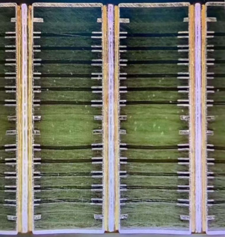
Multilayer PCBs contain three or more conductive copper layers laminated between insulating dielectric materials. What makes this revolutionary? The vertical stacking enables complex routing that would require multiple separate boards in conventional designs. Standard configurations range from 4-layer consumer electronics to 48-layer supercomputing applications.
The construction alternates conductive and insulating layers with prepreg bonding material. Here’s the technical detail: Microvias as small as 15µm now connect layers in high-density designs, while advanced materials like Rogers 4350B handle 5G frequencies up to 77GHz.
| Parameter | Multilayer PCB | Standard PCB |
|---|---|---|
| Layer Count | 4-50+ | 1-2 |
| Trace Width | 25-100µm | 100-300µm |
| Via Size | 15-200µm | 300-500µm |
| Signal Layers | Dedicated planes | Shared layers |
Fabricating multilayer boards requires precision engineering. The process begins with inner layer imaging using direct laser plotting at 20,000 DPI resolution. After etching, layers undergo automated optical inspection before oxide treatment enhances bonding strength.
Here’s where it gets complex: The lamination process applies 300 psi pressure at 180°C for FR4 materials. High-reliability applications use sequential lamination with multiple press cycles. Post-lamination, laser drills create microvias with positional accuracy under 5µm.

Black PCB Board
Multilayer technology solves critical electronic challenges. The primary benefit? Space reduction up to 70% versus equivalent single-layer designs. Other advantages include:
● 40dB better EMI shielding
● 5x improved signal integrity
● 60% weight reduction
● Enhanced thermal dissipation
While powerful, these boards present unique challenges. The main constraints include 3-5x higher fabrication costs and 50% longer lead times versus standard PCBs. Design complexity requires specialized EDA tools with 3D modeling capabilities.
These boards enable mission-critical applications. Leading sectors include:
● Telecommunications (5G mmWave equipment)
● Automotive (ADAS radar systems)
● Aerospace (satellite payloads)
● Medical (MRI machines)
Choosing layers involves careful analysis. The rule of thumb: Add signal layers when trace density exceeds 120cm/cm². Power integrity requirements often dictate separate ground and power planes.
Material selection impacts all parameters. High-frequency designs require Rogers RO4000 with εr=3.38, while thermal-intensive applications use aluminum cores with 5W/mK conductivity.
Controlled impedance is critical. The formula: Z₀=√(L/C) where L=inductance and C=capacitance. Stackups require precise dielectric spacing to maintain ±5% tolerance.
High-density interconnect pushes boundaries. Cutting-edge features include:
● Stacked microvias
● Any-layer interconnects
● 15µm line/space
● Embedded passives
Avoid these frequent errors:
● Inadequate power plane stitching
● Improper via transition zones
● Neglecting manufacturability rules
● Insufficient thermal relief
Quality assurance involves multiple methods. Automated optical inspection checks 100% of surfaces, while flying probe testing verifies electrical continuity. Environmental stress screening includes:
● Thermal cycling (-55°C to +125°C)
● Vibration testing (20-2000Hz)
● Humidity exposure (85°C/85% RH)
Pricing depends on multiple factors:
● Layer count (40% of cost)
● Materials (25%)
● Via technology (15%)
● Testing (10%)
● Finish type (10%)
Emerging technologies include:
● 3D printed electronics
● Embedded active components
● AI-optimized routing
● Sustainable materials
Vet suppliers thoroughly. Key qualifications:
● IPC-6012 Class 3 certification
● ITAR registration
● 10+ years experience
● 99.5% on-time delivery
Multilayer technology continues evolving. Next-generation developments focus on heterogeneous integration combining silicon interposers with organic substrates.
Q1: What’s the practical layer limit?
Current technology maxes at 50 layers, though most applications use 4-16 layers.
Q2: How do multilayer PCBs handle heat?
Thermal vias, metal cores, and strategic component placement dissipate heat effectively.
Q3: Can I prototype multilayer boards?
Yes, but expect 3-4 week lead times versus 1 week for production.
Q4: What design software works best?
Altium, Cadence, and Mentor Xpedition offer advanced multilayer capabilities.
Q5: Are there eco-friendly options?
New halogen-free and recyclable materials reduce environmental impact.
This comprehensive guide covers all aspects of multilayer PCB technology. For implementation support, consult with certified PCB design specialists to optimize your specific application requirements.


Connect to a Jerico Multilayer PCB engineer to support your project!
Request A Quote


 Quote
Quote