


+86 13603063656
PCB board manufacturing is an essential process for the creation of electronic devices, powering everything from smartphones to medical devices. The complexity of the process ensures that high-quality PCBs meet the performance, reliability, and cost standards required by industries across the board. This article aims to provide an in-depth exploration of PCB board manufacturing, highlighting the steps involved, materials used, and how businesses can optimize their PCB production to meet their specific needs. If you’re looking to understand how PCB manufacturing impacts your products and how to get the most out of it, you’re in the right place.

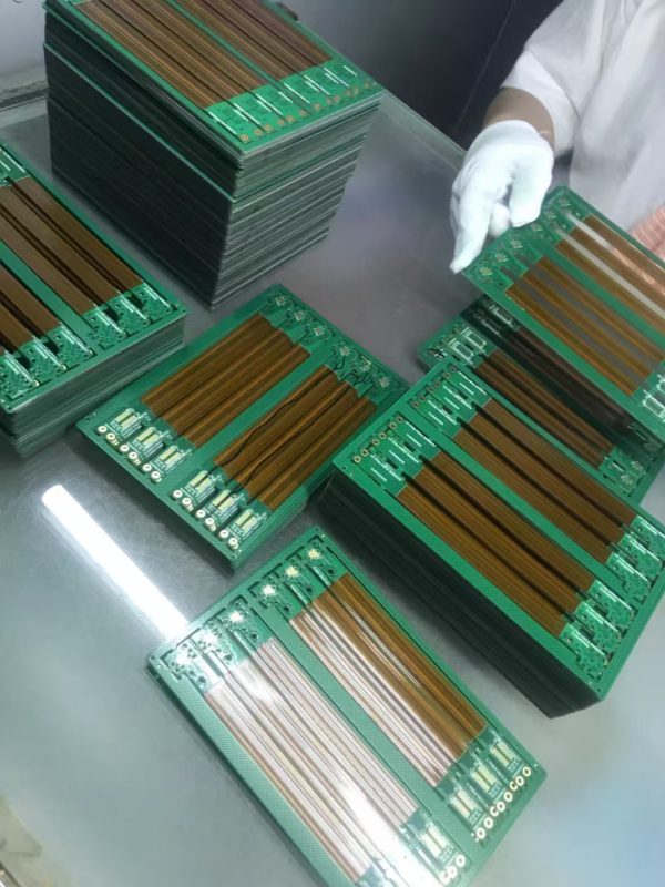
PCB Board Manufacturing
PCB board manufacturing is the process of creating printed circuit boards, which are the backbone of modern electronic devices. What’s the real story? Without PCBs, many of the devices we rely on wouldn’t function properly. From smartphones to computers, the boards serve as the essential support for the electrical components of every device.
The manufacturing process of PCBs involves a series of steps starting from design and fabrication, to assembly and testing. The quality of the PCB directly impacts the performance of the final product, which is why it’s crucial to choose the right manufacturing process. Understanding how the process works, from the raw materials used to the testing stages, can help businesses make informed decisions about their PCB production needs.
Table 1: Key Steps in PCB Board Manufacturing
| Step | Description | Key Tools and Equipment |
|---|---|---|
| Design | Creating the circuit layout and specifications | PCB design software (Altium, Eagle) |
| Fabrication | Creating the physical PCB from raw materials | CNC machines, etching tanks |
| Assembly | Placing and soldering components | Pick-and-place machines, soldering stations |
| Testing | Ensuring the PCB works as expected | AOI machines, functional testers |
PCB manufacturing isn’t a one-size-fits-all process. But here’s the kicker: there are several types of PCBs, each requiring a unique manufacturing approach. Let’s explore the most common types of PCBs and the specific requirements needed to produce them.
Table 2: Types of PCBs and Their Requirements
| PCB Type | Description | Manufacturing Complexity | Common Applications |
|---|---|---|---|
| Single-layer PCBs | Simple design, one conductive layer | Low | Consumer electronics, toys |
| Multi-layer PCBs | Multiple layers for complex circuits | High | Smartphones, computers |
| Flexible PCBs | Made from flexible materials, bends without breaking | High | Wearables, foldable displays |
| Rigid-flex PCBs | Combination of rigid and flexible PCBs | Very High | Aerospace, robotics |
| HDI PCBs | High-density circuits with fine interconnects | Very High | Medical devices, high-speed electronics |
PCB manufacturing involves several steps, each of which plays a critical role in the final product’s quality and performance. Ready for the good part? Let’s break down the process from start to finish.
The first step in PCB manufacturing is design. Using specialized PCB design software, engineers create a blueprint for the board, including the layout of the circuits and components. Once the design is finalized, it is converted into files that will be used during the fabrication process.
Next, in the fabrication stage, the raw materials, typically copper-clad laminates, are cut to size. The copper is then etched away using chemicals or lasers to create the electrical pathways. Depending on the design, the board may also undergo multiple layers, where each layer is etched and stacked carefully to create the final multi-layer PCB.
Once the board is fabricated, assembly follows. This involves placing the components, like resistors, capacitors, and chips, onto the PCB and soldering them in place. This can be done manually or using automated pick-and-place machines, depending on the complexity and scale of the production.
Finally, the testing phase ensures that the PCB functions as intended. This can involve functional testing, automated optical inspection (AOI), or X-ray inspection to detect any hidden defects. Boards that pass testing are ready for delivery or integration into the final product.
Table 3: PCB Manufacturing Process Breakdown
| Step | Key Tasks | Tools and Techniques |
|---|---|---|
| Design | Creating the schematic layout | PCB design software (e.g., Altium) |
| Fabrication | Etching and drilling the PCB | CNC machines, chemical etching |
| Assembly | Soldering components onto the PCB | Pick-and-place, reflow soldering |
| Testing | Checking functionality and inspecting the board | AOI, X-ray, functional testing |
Designing a PCB is arguably the most important part of the entire manufacturing process. What’s the real story? The design directly influences the performance, reliability, and cost of the final product.
Good PCB design involves laying out the electrical components and creating the pathways that will connect them. Design software like Altium Designer or Eagle is used to create a digital representation of the board. During this phase, engineers must ensure that the design minimizes the risk of issues like signal interference, power loss, and overheating.
The design also needs to account for manufacturability. This includes choosing the right materials, specifying the board’s dimensions, and ensuring the board can be efficiently assembled. During this phase, engineers must also decide on factors like the number of layers, component placement, and trace width.
Table 4: PCB Design Considerations
| Consideration | Description | Importance |
|---|---|---|
| Trace Width | The width of the electrical pathways | Affects current handling and performance |
| Layer Count | Number of layers in the PCB | Affects complexity and cost |
| Component Placement | Positioning of components on the board | Impacts functionality and space efficiency |
| Material Selection | Choice of PCB material | Affects durability and cost |
The materials used in PCB manufacturing play a huge role in the performance and cost of the final product. Ready for the good part? Let’s explore the most commonly used materials in PCB production and their specific advantages.
Each material has its own set of advantages and is chosen based on the specific requirements of the application. Understanding the material options available can help businesses make more informed decisions about their PCB manufacturing needs.
Table 5: Common PCB Materials
| Material | Properties | Common Applications |
|---|---|---|
| FR4 | Strong, cost-effective, and durable | Consumer electronics, automotive |
| Aluminum | Excellent heat dissipation | LED lighting, power electronics |
| Ceramic | High thermal conductivity | High-frequency, medical devices |
| Polyimide | Flexible and durable | Wearables, foldable displays |
The fabrication process is where the raw materials come to life. Let’s take a deep dive into the key steps involved in PCB fabrication and what makes them so important.
The first step in the fabrication process is material preparation, where copper-clad laminate is cut to the required size. The laminate serves as the base material for the PCB. The etching process follows, where the copper is selectively removed to form the electrical traces.
Next comes drilling, where holes are created for through-hole components and vias that connect different layers of the PCB. The drilling process must be precise to ensure the accuracy of the final board.
Once drilling is complete, the PCB undergoes plating, where a layer of metal is deposited onto the holes to create electrical connections. The final step is cleaning and testing, ensuring that the board is free from defects and ready for assembly.
Table 6: PCB Fabrication Steps
| Step | Description | Tools Used |
|---|---|---|
| Material Preparation | Cutting the laminate to the required size | CNC machines |
| Etching | Removing unwanted copper to form circuits | Chemical etching tanks |
| Drilling | Creating holes for components and vias | CNC drilling machines |
| Plating | Depositing metal onto holes | Electroplating systems |
| Cleaning | Removing residue and testing for defects | Cleaning tanks, AOI machines |
Assembly is where the components are placed onto the PCB to form a complete circuit. But here’s the kicker: this is the stage where precision really matters.
PCB assembly can be done in one of two ways: Through-Hole Technology (THT) or Surface Mount Technology (SMT). THT involves inserting components with leads through holes in the PCB and soldering them in place. This method is typically used for larger components that require stronger mechanical support. SMT, on the other hand, involves mounting smaller components directly onto the surface of the PCB. SMT is faster and more efficient, making it ideal for high-volume production.
For high-quality assembly, automated systems such as pick-and-place machines are used to place components with precision. After components are placed, the board is soldered using wave soldering (for THT components) or reflow soldering (for SMT components).
Table 7: THT vs. SMT Assembly Comparison
| Feature | THT Assembly | SMT Assembly |
|---|---|---|
| Component Size | Larger components with leads | Smaller components, no leads |
| Assembly Speed | Slower, more labor-intensive | Faster and more automated |
| Mechanical Strength | Stronger mechanical support | Lower strength, but sufficient for most applications |
| Cost | Higher due to labor and equipment | Lower due to automation and material efficiency |
Testing and quality control are crucial to ensure that the PCB functions as intended. Ready for the good part? Let’s look at the various methods used to test PCBs during manufacturing and why they matter.
One of the most common testing methods is Automated Optical Inspection (AOI). This method uses cameras to visually inspect the PCB for defects like misalignment, missing components, or soldering errors. AOI is fast and accurate, making it ideal for high-volume production.
Another important test is In-Circuit Testing (ICT), which checks the electrical connections of the PCB. ICT involves probing the board to measure resistance and continuity, ensuring that all connections are properly made.
Finally, Functional Testing is performed to simulate the actual operation of the PCB within its intended device. This test verifies that the board performs as expected and is free from any functional defects.
Table 8: PCB Testing Methods
| Test Type | Purpose | Benefits |
|---|---|---|
| AOI | Visual inspection for defects | Fast, high-accuracy defect detection |
| ICT | Checking electrical connections and resistance | Verifies proper functionality |
| Functional Testing | Simulating the final operation of the PCB | Ensures the board meets performance requirements |
Advancements in PCB technology continue to push the boundaries of what is possible in electronics. What’s the real story? New techniques are enabling the creation of more compact, powerful, and efficient PCBs.
One of the most exciting developments is the use of HDI (High-Density Interconnect) technology. HDI PCBs allow for more complex and compact designs, enabling devices to become smaller while still offering high-performance capabilities. This is particularly useful for mobile phones, wearables, and other compact electronics.
Laser drilling has also revolutionized the PCB manufacturing process. Laser drilling allows for more precise hole creation, enabling the use of finer traces and higher-density components. This is critical for producing advanced multi-layer PCBs that require very fine and accurate holes.
Lastly, 3D printed PCBs are beginning to emerge as a promising option for low-volume, high-precision manufacturing. These PCBs are built layer by layer, making them suitable for complex and custom designs.
Table 9: Advanced PCB Technologies
| Technology | Description | Benefits |
|---|---|---|
| HDI PCBs | High-density interconnects for compact designs | Enables smaller, more powerful devices |
| Laser Drilling | Precision drilling using lasers | Allows for fine traces and higher density |
| 3D Printed PCBs | Additive manufacturing of PCBs | Suitable for custom designs and prototypes |
As environmental concerns rise, the PCB manufacturing industry is shifting toward more sustainable practices. Ready for the deep dive? Let’s explore how manufacturers are becoming more eco-friendly and why it matters.
One of the most significant shifts in the industry is the move towards lead-free solder. Traditional solder often contains lead, a toxic substance that can cause environmental harm when disposed of improperly. Lead-free solder is now a standard in PCB manufacturing, helping reduce the environmental impact.
Moreover, PCB recycling is gaining traction as manufacturers look for ways to reuse precious metals like gold, silver, and copper from old PCBs. This not only helps conserve resources but also reduces the amount of electronic waste that ends up in landfills.
Table 10: Environmental PCB Practices
| Practice | Description | Impact on the Environment |
|---|---|---|
| Lead-Free Solder | Solder without lead, using alternative alloys | Reduces toxic waste and improves recyclability |
| PCB Recycling | Reusing precious metals from old PCBs | Decreases electronic waste and saves resources |
| Eco-Friendly Materials | Using biodegradable and recyclable materials | Minimizes the environmental footprint of manufacturing |
In conclusion, PCB board manufacturing is a critical process that impacts the quality, reliability, and cost of your electronic products. By understanding the various steps involved, from design and fabrication to assembly and testing, businesses can ensure they select the right manufacturing partners and materials for their projects. Ready for the good part? By optimizing your PCB manufacturing process, you can reduce costs, improve performance, and stay ahead of the competition in the fast-paced world of electronics.
FAQ Section
Q1: What is PCB board manufacturing?
A1: PCB board manufacturing is the process of creating printed circuit boards used in electronic devices. It involves design, fabrication, assembly, and testing to ensure the board meets required performance and quality standards.
Q2: How does the PCB manufacturing process work?
A2: The PCB manufacturing process starts with design, followed by fabrication (etching, drilling), assembly (soldering components), and testing (inspection, functional tests) to ensure the final product meets the required specifications.
Q3: What are the different types of PCBs?
A3: The different types of PCBs include single-layer, multi-layer, flexible, rigid-flex, and HDI PCBs. Each type has specific manufacturing requirements based on the complexity and function of the board.
Q4: Why is PCB design important?
A4: PCB design is crucial because it sets the foundation for the PCB’s functionality, performance, and manufacturability. A well-designed PCB ensures reliable operation and minimizes potential defects.
Q5: How can PCB manufacturing be environmentally friendly?
A5: PCB manufacturing can be more eco-friendly by using lead-free solder, recycling old PCBs to recover precious metals, and using biodegradable or recyclable materials to reduce waste and environmental impact.


Connect to a Jerico Multilayer PCB engineer to support your project!
Request A Quote


 Quote
Quote