


+86 13603063656

The PCB board manufacturing process stands at the heart of every modern electronics innovation. But here’s the kicker… without a precise, reliable, and high-quality process, even the most ingenious product design can flop. This guide explores the entire pcb board manufacturing process from concept to final inspection. We’ll walk you through every step, from initial design to the latest trends, revealing how each stage contributes to quality, cost efficiency, and consistent results for your B2B operation. Whether you’re an OEM, an engineering manager, or a procurement professional, you’ll discover actionable insights that streamline your workflow and boost your bottom line.
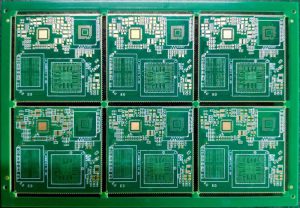
PCB Board Manufacturing Process
Before a single board is fabricated, the journey starts with design and engineering preparation. Ready for the good part? This phase isn’t just about creativity; it’s where mistakes cost the least and savings add up fast. Engineers create schematic diagrams, mapping out how each component connects. Layout designers translate schematics into precise patterns using CAD tools, ensuring clear trace routing, optimal component placement, and signal integrity. Here’s the real story: design for manufacturability (DFM) reviews at this stage can prevent rework and delays down the line.
Designers must generate Gerber files, drill data, and Bills of Materials (BOM), which serve as the digital blueprint for fabrication. Leading PCB manufacturers provide DFM checks that highlight issues like trace width violations, via misplacement, or pad size mismatches. For example, a North American medical device company cut prototyping time in half by integrating early DFM checks, while an automotive supplier reduced return rates by catching potential design flaws before production. Industry data shows that 80% of PCB manufacturing problems stem from design errors—a simple DFM check can slash defect rates by more than 60%.
| Task | Purpose | Typical Software/Tools |
|---|---|---|
| Schematic Capture | Electrical connections | Altium, OrCAD, Eagle |
| PCB Layout | Physical trace and pad placement | Altium, Mentor Graphics |
| DFM Review | Ensure manufacturability | Valor, Zuken |
| Gerber/Drill Generation | Digital manufacturing files | CAM350, ViewMate |
| BOM Creation | List of required components | Excel, Arena, ERP tools |
What’s the real story? Your choice of printed circuit board material can make or break performance. The pcb board manufacturing process relies on substrates like FR4 for general electronics, aluminum for high-power LEDs, and polyimide for flexible circuits. Each material impacts thermal conductivity, dielectric strength, and cost. Copper foil thickness (measured in ounces per square foot) determines current capacity and trace durability. Let’s not forget: specialty laminates such as Rogers or Teflon are used in high-frequency or RF designs for their low signal loss.
For example, a telecom OEM upgraded to high-Tg FR4 to solve thermal failures in 5G base stations. Meanwhile, an EV battery maker switched to heavy copper boards, boosting reliability under high current loads. Material choice also affects compliance—many automotive and medical PCBs must meet UL 94V-0 flame retardancy and RoHS/REACH environmental regulations. The right combination reduces failures, supports your application needs, and aligns with your customer requirements.
| Material | Properties | Best Use Cases | Cost Level |
|---|---|---|---|
| FR4 | Standard, affordable, good all-around | Consumer electronics, industrial | $ |
| Aluminum | High thermal conductivity | Power, LEDs | $$ |
| Polyimide | Flexible, high-temp resistant | Flex circuits, aerospace | $$$ |
| Rogers/Teflon | Low loss, high frequency | RF/microwave, telecom | $$$$ |
Layer stack-up is where the magic of miniaturization meets the brute force of physics. But here’s the kicker… the right stack-up controls crosstalk, EMI, and power distribution—essential in the pcb board manufacturing process. Designers choose single, double, or multilayer PCBs based on circuit complexity. High-speed data lines, like those in server backplanes, demand controlled impedance, so careful dielectric thickness and layer sequence planning are critical.
For instance, a global networking company resolved EMI issues by introducing ground planes between signal layers, while an industrial controls manufacturer reduced board warpage by balancing layer symmetry. Signal integrity simulations (using tools like HyperLynx or SIwave) predict problems before they happen. Layer stack-up isn’t just a technical detail—it’s a cost driver, impacting everything from material selection to lamination cycles.
| Layer Count | Structure Example | Typical Application |
|---|---|---|
| 1–2 | Signal layers only | Simple consumer, LED, power |
| 4 | Signal, ground, power, signal | Automotive, industrial controls |
| 6–12 | Signal, power, multiple grounds | Networking, telecom, aerospace |
| 14+ | Custom stack, HDI | Advanced server, high density |
Ready for the good part? This is where your printed circuit board comes to life—inner layers are coated with photoresist, exposed to UV light through a mask, and developed to reveal the intended copper pattern. Chemical etching then removes unwanted copper, leaving behind only the desired traces. Accuracy is everything: a 10 μm misalignment at this stage can render a $50,000 production run useless.
A leading smartphone maker improved yield by implementing real-time imaging checks and automated etch bath monitoring, slashing scrap rates by 30%. Meanwhile, defense contractors use double-sided AOI (Automated Optical Inspection) to guarantee 100% trace integrity on all internal layers. But here’s the kicker… trace defects that go unnoticed now can cause shorts, opens, or crosstalk later. Investing in imaging and etching precision is non-negotiable in any serious pcb board manufacturing process.
| Process Step | Key Tools/Equipment | Critical Control |
|---|---|---|
| Photoresist Application | Lamination machine | Thickness, cleanliness |
| UV Exposure | UV exposure units | Alignment accuracy |
| Development | Developer tank | Timing, resist removal |
| Etching | Etchant bath | Concentration, duration |
| AOI Inspection | Optical scanner | Pattern matching |
But here’s the kicker… if your printed circuit board layers aren’t perfectly aligned and bonded, the entire pcb board manufacturing process is at risk. Lamination presses inner and outer layers together with prepreg (uncured resin) under high heat and pressure. Multilayer PCBs may contain up to 20 layers—each must be registered within ±0.05mm to avoid warpage or electrical faults.
Real-world example: a German automotive supplier reduced field failures by switching to vacuum-assisted lamination, eliminating voids and delamination. In Asia, a medical device firm improved reliability by adopting prepreg with higher glass content, which resisted resin flow and maintained layer integrity. Lamination failures account for over 40% of multilayer PCB defects, according to IPC data, making this step a vital checkpoint for quality.
| Parameter | Typical Range | Impact |
|---|---|---|
| Temperature | 160°C – 200°C | Curing, layer bonding |
| Pressure | 10 – 25 bar | Resin flow, registration |
| Time | 45 – 90 minutes | Complete curing |
| Vacuum Assist | Yes/No | Void elimination |
Ready for the good part? Drilling is more than poking holes—it’s a high-precision process that affects everything from assembly yield to board performance. Automated CNC drills or lasers create via holes and through-holes, with tolerances often tighter than ±0.05mm. Blind and buried vias in HDI PCBs demand multiple drill passes and x-ray alignment for accuracy.
Case study: a leading EV manufacturer switched to laser microvia drilling, increasing routing density and cutting board size by 15%. Meanwhile, a contract manufacturer improved first-pass yield by implementing real-time drill bit monitoring, reducing breakage and misregistration. But here’s the kicker… drill debris and burrs can cause open circuits and solderability issues if not controlled, so post-drill cleaning is standard in the pcb board manufacturing process.
| Via Type | Description | Application |
|---|---|---|
| Through-Hole | Connects all layers | Standard PCBs |
| Blind Via | Connects outer to inner | HDI, compact designs |
| Buried Via | Connects inner layers only | Multilayer, high-density |
| Microvia | Laser-drilled, tiny | Smartphones, RF modules |
But here’s the kicker… copper plating is what makes your vias and through-holes conduct electricity reliably. The pcb board manufacturing process uses electroless copper for initial deposition, followed by electrolytic plating to thicken the copper walls. A typical board aims for 20–25 μm copper thickness in holes for durability and low resistance.
For example, an aerospace company slashed field returns by implementing advanced bath filtration, eliminating contaminant-driven voids. In Europe, a telecom board maker used pulse-plating technology to achieve ultra-uniform copper distribution, key for high-speed signals. The cost of inadequate plating? According to IPC, nearly 70% of in-field PCB electrical failures trace back to plating or via integrity issues.
| Step | Purpose | Key Metrics |
|---|---|---|
| Electroless Copper | Initial thin copper layer | Adhesion, coverage |
| Electrolytic Plating | Build copper thickness | Uniformity, thickness |
| Final Rinse | Remove chemicals | Cleanliness |
| Thickness Testing | Measure via/trace copper | 20–25 μm typical |
Now it’s time for the outer layers—the showpieces of your printed circuit board. Ready for the good part? Photoresist is applied, exposed, and developed just as for the inner layers, but even tighter tolerances matter for SMT and fine-pitch BGA pads. Outer layer etching is closely monitored; even a 5 μm over-etch can make a difference in high-frequency or impedance-controlled circuits.
A leading telecom manufacturer solved signal loss issues by switching to direct-imaging for outer layers, boosting yield by 22%. A Chinese LED company cut rework costs with inline AOI after etching, catching shorts before assembly. The big lesson? Outer layer precision is essential to modern high-speed, high-density pcb board manufacturing process.
| Step | Key Focus | Typical Tolerance |
|---|---|---|
| Photoresist | Thickness, uniform | ±2 μm |
| Exposure | Alignment | ±5 μm |
| Etching | Width, edge control | ±10 μm |
| AOI | Short, open detection | 99%+ coverage |
Here’s where it gets interesting… the solder mask is the unsung hero of the pcb board manufacturing process, preventing solder bridges and protecting copper. It’s applied as a liquid or dry film, then UV-cured. Mask openings must align perfectly to expose only the pads and vias that need to be soldered—no more, no less.
One U.S. audio equipment firm reduced assembly defects by switching to LPI (Liquid Photo-Imageable) solder mask, which offers superior alignment and reliability. An Asian contract manufacturer found that improved mask thickness standards cut solder shorts by 40%. Mask color isn’t just cosmetic—green, blue, black, and white all have distinct properties for reflectivity and inspection.
| Mask Type | Pros | Cons | Typical Use |
|---|---|---|---|
| LPI (Liquid) | High precision, durable | Costlier, requires imaging | Most common |
| Dry Film | Simple for basic PCBs | Less precise, hard to rework | Legacy/cheap |
| Colors | Inspection, heat, light | Process adjustments | Application-based |
Ready for the good part? The silkscreen (legend) adds vital information—component IDs, polarity marks, logos—directly to the printed circuit board surface. Silkscreen printing can be done by screen, inkjet, or laser, with white ink on green solder mask being the most readable. Poor legend quality leads to assembly errors and increases manual inspection costs.
For example, a U.S. contract assembler reduced their placement mistakes by 30% after switching to high-res inkjet silkscreening. Meanwhile, an IoT startup cut rework time by implementing barcode legends, allowing automatic scanning for assembly traceability. But here’s the kicker… silkscreen ink must be heat-stable and resistant to cleaning agents; otherwise, you risk fading during reflow or wash.
| Printing Method | Benefits | Typical Issues |
|---|---|---|
| Screen Print | Cost-effective, thick | Less resolution |
| Inkjet Print | High-res, flexible | Ink adhesion |
| Laser Marking | Durable, permanent | Slow for volume |
| Color Choices | Green/white best | Readability varies |
But here’s the kicker… without a proper surface finish, even the best board will fail in assembly. Surface finishes protect exposed copper, improve solderability, and can extend shelf life. Common finishes include HASL (Hot Air Solder Leveling), ENIG (Electroless Nickel Immersion Gold), OSP (Organic Solderability Preservative), Immersion Silver, and Tin.
A Swiss industrial electronics firm switched from HASL to ENIG for a medical project, reducing solder joint failures and meeting strict reliability standards. Meanwhile, an LED lighting producer adopted OSP to cut costs while still passing RoHS compliance. What’s the real story? Each finish has trade-offs in flatness, cost, and compatibility with lead-free soldering.
| Finish | Advantages | Drawbacks | Best Applications |
|---|---|---|---|
| HASL | Inexpensive, robust | Uneven, not fine pitch | Industrial, consumer |
| ENIG | Flat, long shelf life | Costly, brittle Ni | Medical, fine-pitch SMT |
| OSP | Cheap, flat, eco-friendly | Short shelf life | Mass-market, RoHS |
| Imm Silver | Flat, good for RF | Tarnish risk | Telecom, RF |
| Imm Tin | Lead-free, flat | Whiskers, shelf life | Automotive, general |
This is where it gets interesting… the pcb board manufacturing process is only as good as its test strategy. Every board undergoes electrical testing—flying probe or bed-of-nails fixtures check for opens, shorts, and, in advanced cases, controlled impedance. High-value applications often demand 100% net testing; for instance, server and aerospace PCBs must log every test for traceability.
A contract assembler saw a 99.8% first-pass yield after implementing statistical test data analysis. Meanwhile, a telecom company cut warranty claims by 20% by using impedance-controlled testing on every run. But here’s the kicker… testing is a final insurance policy. Boards failing test are flagged for rework or scrapped, not shipped.
| Test Type | What It Checks | Ideal For |
|---|---|---|
| Flying Probe | Opens/shorts, all nets | Prototype, low-volume |
| Bed-of-Nails | Fast, all nets | High-volume, repeat |
| Impedance Test | Signal integrity | RF, telecom, high-speed |
| Burn-In | Long-term stress | Aerospace, defense |
Ready for the good part? The last stage is cutting, routing, and the all-important final inspection. printed circuit boards are profiled using routers, V-scores, or punches to achieve their final shape. Edges must be smooth, and features like slots and cutouts precisely milled. What’s the real story? Poor routing can leave burrs, delaminate layers, or break traces—serious risks for assembly and use.
After routing, boards go through AOI and human inspection. A leading industrial controls manufacturer cut their customer complaints in half by adding automated mechanical testing for edge strength. Packing is no afterthought—antistatic bags, vacuum sealing, and custom foam keep boards safe in transit. The process ends only when the product reaches your dock intact and ready for the next step.
| Profiling Method | Use Case | Tolerance |
|---|---|---|
| Routing | Custom shapes, slots | ±0.1 mm |
| V-Scoring | Snap-apart panels | ±0.15 mm |
| Punching | Simple, high-volume | ±0.2 mm |
| Inspection Steps | AOI, manual, mechanical | IPC-6012 |
But here’s the kicker… the pcb board manufacturing process is evolving fast. Automation, Industry 4.0, and big data are streamlining everything from DFM to traceability. Robotics are cutting labor costs by 40% in some Asian factories. Advanced AOI now uses AI to spot pattern deviations invisible to the human eye.
A top automotive supplier reduced field recalls by integrating IoT sensors in every production stage, creating real-time process feedback. Eco-friendly materials and closed-loop chemical management are cutting waste and meeting tough global regulations. Here’s the real story: PCB factories adopting these trends are achieving defect rates below 300 ppm and blazing new trails in quality and efficiency.
| Trend/Tech | Benefit | Current Adoption |
|---|---|---|
| Automation/Robotics | Lower costs, higher quality | Growing rapidly |
| AI-Powered AOI | Higher detection accuracy | High in Tier 1 |
| IoT Traceability | Real-time process control | Leading factories |
| Green Chemistry | Less waste, eco-friendly | Growing in EU/Asia |
The pcb board manufacturing process is more than just a series of technical steps—it’s the backbone of product quality and business competitiveness in the electronics industry. From meticulous design and material selection to layer stack-up, imaging, and precision drilling, every phase matters. But here’s the kicker… embracing innovation and best practices at each stage pays off in reliability, compliance, and customer satisfaction. Ready for the good part? Partnering with expert manufacturers who invest in quality systems and technology will keep your supply chain strong, your costs in check, and your products at the top of their game.
Q1: What is the PCB board manufacturing process?
The PCB board manufacturing process covers all the steps required to turn a design into a functioning circuit board, including design, material selection, layer imaging, etching, drilling, plating, solder masking, finishing, electrical testing, and final inspection.
Q2: How does the PCB lamination process work?
PCB lamination presses multiple layers together using heat and pressure. Prepreg material bonds the layers, ensuring electrical connectivity and mechanical strength. Precise registration is critical to avoid defects.
Q3: What materials are commonly used in PCB manufacturing?
FR4, aluminum, and polyimide are the most common. Specialty substrates like Rogers are used for high-frequency or demanding environments. Copper foil thickness and finish selection impact performance and cost.
Q4: Why is electrical testing important in PCB manufacturing?
It detects open circuits, shorts, and performance issues before assembly, ensuring the printed circuit board will work reliably in its end application and reducing costly failures.
Q5: What are some common quality standards for PCB manufacturing?
Standards like IPC-6012, UL, and RoHS/REACH govern aspects such as board quality, safety, and environmental compliance. Adhering to these standards ensures global marketability and consistent performance.


Connect to a Jerico Multilayer PCB engineer to support your project!
Request A Quote


 Quote
Quote