pcb board meaning—short for Printed Circuit Board—is an essential component in the world of electronics. It provides the mechanical support and electrical pathways for connecting components within a circuit. Understanding what PCB boards are, how they function, and why they’re crucial in electronic devices is fundamental for engineers, manufacturers, and even enthusiasts. Let’s take a closer look at everything you need to know about PCB boards, their design, and their applications.
pcb board meaning
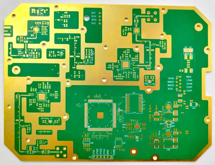
PCB boards are the foundation of modern electronics. Whether you’re looking at your smartphone, computer, or even automotive components, the PCB plays a critical role in the functionality of these devices. But what exactly is a PCB board?
A Printed Circuit Board (PCB) is a flat, rigid or flexible surface made from non-conductive materials like fiberglass, on which conductive copper tracks are etched to form electrical pathways. Components like resistors, capacitors, and chips are soldered onto these copper tracks to form a complete circuit.
PCB boards come in many variations, including single-sided, double-sided, and multi-layer designs, each offering specific benefits depending on the application. Whether you’re designing a simple circuit or developing a complex multi-layer board for a sophisticated electronic device, understanding how PCB supplier made PCB boards and used is essential.
PCB boards consist of several layers that serve specific functions, depending on the design and complexity of the board. Let’s break it down.
● Substrate Layer: The base material that provides structure. Common substrates include fiberglass, which is reinforced with epoxy.
● Copper Layer: Conductive copper is applied on one or both sides of the substrate. This is the layer where the electrical pathways are etched.
● Solder Mask: The protective layer applied over the copper, which prevents short circuits and ensures that only the desired components are soldered onto the copper.
● Silkscreen Layer: This final layer contains the component labels, markings, and other important text to help in assembly and maintenance.
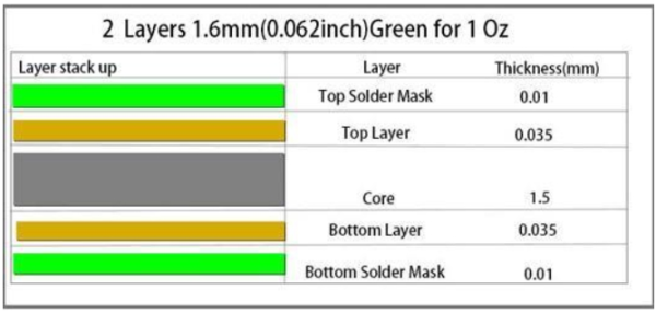
2 Layers PCB Structure
PCBs are classified based on the number of layers they contain:
● Single-Sided PCB: A simple design where all components are placed on one side of the board, and the copper tracks are on the other.
● Double-Sided PCB: Components and copper traces are placed on both sides, providing more routing options.
● Multi-Layer PCB: These boards consist of several layers stacked on top of one another, ideal for complex circuits with high component density.
The manufacturing of PCBs is a multi-step process that includes design, material selection, and assembly. Each step is crucial to ensuring the board meets the required specifications.
The first step in manufacturing a PCB is the design phase. Engineers use specialized PCB design software to create the circuit’s blueprint, which includes the placement of components and routing of electrical traces. The design is then converted into Gerber files that guide the manufacturing process.
Once the design is finalized, the next step is to etch the copper layer. In this step, the copper that is not part of the circuit is chemically removed, leaving behind only the electrical paths.
The board is drilled to make holes for vias (connecting different layers) and through-hole components. These holes are carefully drilled to ensure proper alignment.
Once the holes are drilled, components like resistors, capacitors, and chips are placed on the board and soldered into place. For surface-mount components, automated machines place the components on the board, and a reflow oven melts the solder to establish the connection.
The final step involves rigorous quality control. Automated optical inspection (AOI), electrical testing, and X-ray inspection ensure that the PCB is free from defects and meets electrical standards.
Jerico Multilayer PCB excels in all these phases with their in-house quality control system, experienced engineering team, and precise manufacturing lines that ensure consistently reliable output.
When it comes to PCB designs, there are several types to consider based on the complexity and application needs. Let’s explore the most common types.
This type of PCB has all components mounted on one side, and the electrical pathways are on the other side. Single-sided PCBs are typically used in simple electronic devices like toys, calculators, and basic home appliances.
Double-sided PCBs feature copper traces on both sides of the board. They allow for more complex designs, as components can be placed on both sides of the PCB. Double-sided PCBs are commonly used in power supplies, audio equipment, and communication systems. normally it is an easy pcb
Multi-layer PCBs consist of several layers stacked together to allow for more complex circuitry. These are ideal for devices with high component density, such as smartphones, computers, and medical devices.
Flexible PCBs, or flex PCBs, are used in applications where the PCB needs to bend, twist, or fold. This makes them perfect for wearable electronics, flexible displays, and compact devices where space is limited.
PCB boards are the backbone of every electronic device, from simple home gadgets to sophisticated medical equipment. Here’s why they matter:
PCBs provide a reliable and compact way to arrange and interconnect components. By placing components on a single flat board, the design simplifies manufacturing and reduces the risk of electrical faults.
PCBs allow for high-speed signals to travel efficiently between components. With precise routing and minimal signal interference, PCBs ensure that devices perform at their best.
Once the design is finalized, PCBs can be mass-produced, making them a cost-effective solution for high-volume production. This scalability is particularly beneficial for consumer electronics and other mass-market products.
Designing a PCB requires specialized PCB design software, which provides the tools needed to create the electrical blueprint for a circuit. Let’s explore some of the most popular software options.
● Altium Designer: A professional-grade software used for designing complex, multi-layer PCBs.
● KiCad: A free, open-source option that’s ideal for hobbyists and small-scale projects.
● Eagle: A popular choice for both professionals and enthusiasts, offering powerful features at a lower price point.
PCB design software allows users to create schematics, arrange component footprints, and route electrical paths. The software then generates the Gerber files that guide the manufacturing process, ensuring the PCB is made according to the design specifications.
Once a PCB is manufactured, it’s essential to test and inspect it to ensure it functions correctly. The most common PCB testing methods include:
This ensures that all components are properly connected and the PCB works as intended. Flying probe testing and bed-of-nails testing are common techniques for checking the integrity of the connections.
Automated optical inspection (AOI) is used to visually inspect the PCB for any defects such as soldering issues, component misalignment, or damaged traces.
For multi-layer PCBs, X-ray inspection is used to check the internal layers for issues such as voids, soldering problems, or other structural faults.
High-Density Interconnect (HDI)
Flexible Circuits
Rigid-Flex Structures
These cutting-edge technologies enable thinner, faster, and more compact electronics—something Jerico Multilayer PCB has years of proven experience delivering to global OEM customers.
The process of manufacturing a PCB involves several stages, each contributing to the final product’s quality and functionality. Understanding the steps involved in the PCB manufacturing process is crucial for both designers and manufacturers, as it impacts the performance and reliability of the finished product.
● Design and Layout: The first step involves designing the schematic and creating the layout for the PCB. This phase also includes selecting the appropriate components and materials for the PCB.
● Material Selection: The type of material chosen for the substrate layer plays a significant role in determining the electrical properties and durability of the PCB. Most commonly, FR4 (fiberglass-reinforced epoxy laminate) is used.
● Copper Clad Laminate: Copper is bonded to the substrate to create a base for the circuit pathways. The copper layer thickness can vary based on the design and functionality of the PCB.
● Etching: Once the copper-clad laminate is prepared, the circuit design is transferred to the PCB. Etching removes unwanted copper, leaving behind only the necessary traces to form electrical connections.
● Drilling and Vias: Holes are drilled to create vias, which connect different layers of the PCB. Through-hole components are also placed in these drilled holes.
● Solder Mask Application: A solder mask is applied over the copper traces to prevent short circuits and protect the PCB during soldering. This layer also ensures that only the necessary areas are soldered during component placement.
● Component Placement and Soldering: In this phase, components such as capacitors, resistors, and microchips are mounted onto the PCB using automated machinery. The soldering process solidifies the connections between the components and the copper traces.
● Inspection and Testing: The final step involves inspecting and testing the PCB for quality control. Automated Optical Inspection (AOI) is typically used to detect any faults or irregularities in the PCB design or manufacturing process.
| Stage | Description |
|---|---|
| Design and Layout | Initial stage where the circuit schematic is drawn and layout is planned. |
| Material Selection | Choosing materials for the PCB, including copper and the substrate. |
| Copper Clad Laminate | Bonding copper to the substrate to create the conductive surface for the circuit. |
| Etching | Removal of excess copper to leave behind only the required pathways. |
| Drilling and Vias | Creating holes for vias and through-hole components. |
| Solder Mask Application | Applying a protective layer to prevent shorts and unwanted soldering. |
| Component Placement & Soldering | Placing components on the board and soldering them in place. |
| Inspection and Testing | Quality control procedures like AOI and electrical testing to ensure functionality. |
As PCB technology continues to evolve, manufacturers have introduced advanced techniques to meet the growing demand for smaller, faster, and more reliable electronic devices. Let’s dive into some of these innovative techniques.
HDI PCBs are designed to accommodate high-density components, making them ideal for smartphones, medical devices, and military applications. These boards feature smaller traces, more layers, and finer components than standard PCBs. The ability to pack more components into a smaller area leads to more compact and efficient devices.
Flexible PCBs are made from materials that allow the circuit board to bend, twist, and fold without damaging the electrical pathways. These are used in applications like wearable electronics, automotive systems, and medical devices, where the PCB needs to conform to irregular shapes and limited spaces.
Rigid-flex PCBs combine the durability of rigid PCBs with the flexibility of flexible PCBs. They are commonly used in complex electronic devices where both flexibility and rigidity are needed. These boards are often found in aerospace, military, and high-performance electronics applications.
| Technique | Description |
|---|---|
| High-Density Interconnect (HDI) | Allows for high component density and smaller, more efficient designs. |
| Flexible PCBs | PCBs made from bendable materials, perfect for wearable or space-constrained electronics. |
| Rigid-Flex PCBs | Combines rigid and flexible features for applications needing both flexibility and durability. |
The choice of materials for manufacturing a PCB plays a crucial role in its performance, durability, and cost-effectiveness. Understanding the materials used in PCB production helps in designing a more efficient and reliable PCB.
● FR4 (Fiberglass Reinforced Epoxy): This is the most commonly used material for the PCB substrate, known for its excellent electrical insulation properties and durability.
● CEM1 & CEM3: These are alternatives to FR4, used for less demanding applications. They are typically cheaper but offer lower performance in terms of heat resistance and electrical properties.
● Polyimide: Used for flexible PCBs, polyimide provides excellent thermal stability and flexibility.
● Aluminum: Used primarily in metal-core PCBs for heat dissipation in high-power applications.
● Copper: Copper is the most widely used material for the conductive layer in PCBs due to its excellent electrical conductivity. It can be used in various thicknesses based on the current load requirements.
● Gold: Used for high-reliability applications, gold is often used in surface finishes or for components requiring exceptional corrosion resistance.
● Silver: Silver offers better conductivity than copper but is more expensive and prone to tarnishing.
● Solder Mask: A polymer-based coating applied to the PCB to prevent solder from flowing onto unwanted areas.
● Surface Finish: Surface finishes like HASL (Hot Air Solder Leveling) and ENIG (Electroless Nickel Immersion Gold) provide protection for the exposed copper areas and prevent oxidation.
After the PCB has been manufactured, it undergoes rigorous testing to ensure it functions properly and meets the design specifications. Testing is critical to ensure that the PCB performs as expected in real-world conditions and does not lead to component failures.
● Electrical Testing: Ensures all the electrical pathways on the PCB are functioning properly. Methods like flying probe testing and bed-of-nails testing are commonly used.
● Visual Inspection: Automated Optical Inspection (AOI) is used to visually inspect PCBs for physical defects like misaligned components or broken traces.
● X-Ray Inspection: X-ray technology is used to inspect multi-layer PCBs and ensure the internal layers are correctly aligned and free from defects like voids or soldering issues.
There are several international standards that PCBs must meet before they are considered ready for production. Common standards include:
● IPC-A-600: Specifies the acceptability of printed boards and is commonly used in the industry to ensure high-quality manufacturing.
● IPC-2221: A standard for PCB design, ensuring that the boards meet reliability and performance expectations.
PCB boards are essential components in virtually every electronic device. Their versatility makes them a critical part of numerous industries, from consumer electronics to automotive and medical devices.
PCBs are used in smartphones, computers, televisions, and other household gadgets. In this industry, miniaturization and reliability are key factors in PCB design.
In the automotive sector, PCBs are used in various systems, such as engine control units, sensors, and infotainment systems, where durability and performance are critical.
PCBs in medical devices must meet strict reliability standards. They are used in devices like pacemakers, imaging systems, and diagnostic equipment.
Choosing the right PCB for your project involves evaluating several factors to ensure that it meets your specific requirements. Here’s a guide to help you make the best choice.
● Complexity of the Circuit: For simple circuits, a single-sided PCB may suffice, but more complex designs might require multi-layer PCBs.
● Power Requirements: High-power applications may require a metal-core PCB for better heat dissipation.
● Environmental Factors: For devices exposed to harsh conditions, a PCB with higher thermal resistance and better durability is essential.
It’s important to choose a reputable PCB manufacturer that understands your project’s specific needs. Look for manufacturers who specialize in the type of PCB you require and can meet your quality control standards.
PCBs are the backbone of modern electronics, providing the critical pathways for electrical connections and enabling complex devices to function. From the simplest gadgets to the most sophisticated machinery, the role of PCBs is indispensable. By understanding the design, manufacturing, and testing processes, engineers and manufacturers can create reliable, efficient PCBs that power the future of electronics.
Q1: What exactly is a PCB board?
A: A PCB (Printed Circuit Board) is a rigid or flexible board made of insulating material with copper traces etched onto it. These traces create electrical connections between components, allowing the board to power and control electronic systems in everything from smartphones to industrial machinery.
Q2: Why are PCBs so important in modern electronics?
A: PCBs provide a compact, reliable, and cost-efficient platform to mount and interconnect electronic components. They reduce wiring complexity, ensure consistent performance, and allow for scalable manufacturing of complex circuits.
Q3: What types of PCB boards are commonly used?
A: The most common types are single-sided, double-sided, multi-layer, flexible, and rigid-flex PCBs. The selection depends on the application’s complexity, size constraints, and signal integrity requirements.
Q4: What materials are used to manufacture PCBs?
A: Core materials include FR4 (glass-reinforced epoxy laminate), polyimide (for flexible PCBs), aluminum (for thermal management), and conductive layers made from copper. Surface finishes like ENIG or HASL protect copper and improve solderability.
Q5: What is the difference between SMT and THT assembly?
A: SMT (Surface Mount Technology) places components directly onto the surface of the PCB, allowing high-density layout and automation. THT (Through-Hole Technology) involves inserting leads into drilled holes, offering stronger mechanical bonds—ideal for connectors or large components.
Q6: What are Gerber files, and why are they important?
A: Gerber files are digital design files that define every layer of a PCB—copper traces, drill holes, solder mask, and silkscreen. Manufacturers use these files to precisely fabricate PCBs according to the designer’s specifications.
Q7: How do I choose the right copper thickness for my PCB?
A: Copper thickness depends on current-carrying requirements. Standard PCBs use 1oz copper (≈35μm), while high-power designs may need 2oz or more. Thicker copper also improves thermal performance and mechanical strength.
Q8: How are PCBs tested for quality and reliability?
A: PCBs undergo multiple tests, including electrical testing (continuity and isolation), AOI (automated optical inspection), and X-ray inspection for hidden solder joints or internal layer alignment. This ensures long-term reliability in end-use applications.
Q9: What common factors lead to PCB failure?
A: Failures may result from poor solder joints, inadequate trace width, thermal stress, moisture ingress, or material delamination. That’s why quality materials, precision manufacturing, and proper design practices are critical.
Q10: How do I work with Jerico Multilayer PCB to manufacture my boards?
A: Simply reach out via their official website or request a quote with your Gerber files. Jerico offers expert design support, material consulting, and precision manufacturing—backed by IPC and ISO certifications for reliable performance and fast turnaround.


Connect to a Jerico Multilayer PCB engineer to support your project!
Request A Quote


 Quote
Quote