


+86 13603063656
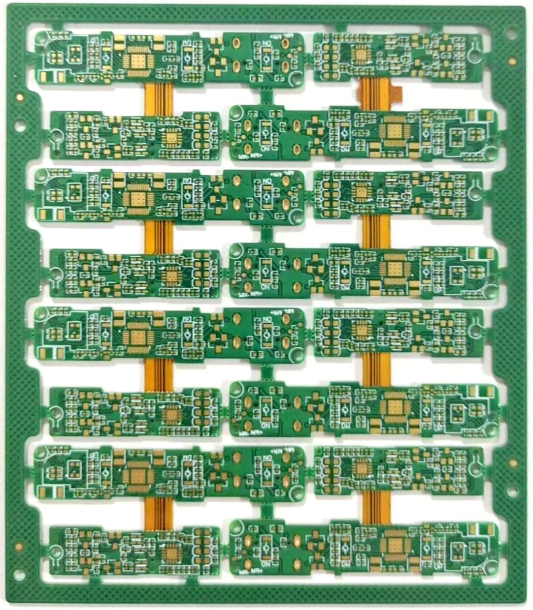
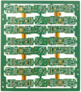
PCB panelization refers to the process of arranging multiple individual PCBs on a single large panel for manufacturing, handling, and testing purposes. This step is crucial in optimizing the PCB production process, reducing costs, and increasing efficiency. By using panelization, manufacturers can streamline their processes and ensure that the final product is reliable and cost-effective. This guide will cover the key aspects of PCB panelization, its types, benefits, and best practices for successful implementation in your PCB production processes.
PCB Panelization
PCB panelization is a fundamental step in the PCB manufacturing process. The idea behind panelization is to create a large sheet or “panel” that holds several individual PCBs. These panels are then processed together, allowing for more efficient use of resources, time, and labor. Panelization also makes it easier to handle multiple PCBs at once, especially when dealing with small or fragile designs. It is particularly important when producing small-run prototypes or when a circuit board design is too complex or small to be manufactured individually.
But here’s the kicker… Panelization not only boosts efficiency but also ensures that each PCB is manufactured consistently and reliably. It minimizes handling errors, maximizes material usage, and facilitates quality control at every stage of production.
| Benefit | Description |
|---|---|
| Cost Efficiency | Reduces material waste and manufacturing time |
| Increased Throughput | Multiple boards are processed simultaneously |
| Simplified Handling | Easier transportation, testing, and assembly |
The PCB panelization process involves several steps that vary depending on the complexity of the design and the manufacturing process. The goal is to combine several individual boards into one larger panel that can be easily processed and then separated later for use in the final product. The process starts with selecting the right panel size and method, which can vary based on the specific project requirements.
What’s the real story? The effectiveness of panelization depends on careful planning at the beginning of the process. Choosing the right panel size, layout, and separation method can significantly impact the efficiency and cost-effectiveness of the manufacturing process.
There are two primary methods for panelizing PCBs: array panelization and linear panelization. Array panelization involves placing multiple boards in a grid-like pattern, while linear panelization arranges the boards in a series of rows, typically used for more straightforward designs.
| Panelization Type | Description | Use Case |
|---|---|---|
| Array Panelization | PCBs arranged in a grid pattern | Complex, high-density designs |
| Linear Panelization | PCBs arranged in rows | Simple, cost-effective designs |
The type of PCB panelization chosen depends on factors such as the PCB design, its size, and the intended use of the final product. While array panelization is ideal for high-density, complex designs, linear panelization is often chosen for simpler, lower-cost designs. The decision on the panelization method impacts manufacturing efficiency, material usage, and product quality.
Ready for the good part? The key to efficient PCB panelization lies in determining the optimal arrangement of your boards within the panel. Depending on the type of PCB, panel size, and complexity, there are several options to consider.
| Type | Description | Use Case |
|---|---|---|
| Single-Sided Panelization | Components placed only on one side of the board | Simple, low-cost designs |
| Double-Sided Panelization | Components placed on both sides of the board | Complex designs with higher component density |
| Multi-Layer Panelization | Multiple layers of PCBs stacked together | High-performance and high-density applications |
The materials used in PCB panelization are critical for ensuring the strength, durability, and functionality of the final product. The most common material for PCBs is FR4 (a type of fiberglass), but other materials, such as aluminum or ceramic, are sometimes used for specific applications like heat dissipation or high-frequency operations.
This is where it gets interesting… The substrate material plays a huge role in the overall performance of the PCB, affecting its electrical properties, thermal management, and even its cost.
The substrate forms the base of the PCB and is typically made from materials like FR4 for standard applications or aluminum for metal core PCBs. The choice of substrate material affects the rigidity, heat dissipation, and electrical properties of the board.
Copper is used to create the conductive traces on the PCB. The thickness of the copper foil determines the board’s ability to handle high current. For panelization, copper foil thickness is chosen based on the power requirements and size of the design.
The solder mask is a protective coating that prevents short circuits during assembly by covering the copper traces. Silkscreen is used for labeling components and marking the PCB for easy identification during assembly.
| Material | Function | Typical Application |
|---|---|---|
| FR4 | Common substrate material, cost-effective | Standard consumer electronics |
| Aluminum | Used for heat dissipation and rigidity | LED lighting, high-power electronics |
| Copper | Conductive material for traces | All types of PCBs |
| Solder Mask | Protective layer to prevent shorts | General-purpose PCBs |
PCB panelization offers several advantages that enhance the efficiency, cost-effectiveness, and reliability of the manufacturing process. By combining multiple boards into a single panel, manufacturers can process them all at once, reducing material waste, labor costs, and the risk of errors.
What’s the real story? Panelization not only improves production efficiency but also makes it easier to handle and test multiple PCBs simultaneously. This step is crucial for achieving a smooth transition from prototype to mass production.
Panelizing PCBs helps reduce material waste by maximizing the use of each substrate. Additionally, handling and processing multiple boards at once reduces labor and testing costs, contributing to overall cost savings.
Panelization allows for greater throughput and faster production. With multiple boards being processed together, manufacturers can scale their operations more effectively and meet production demands more efficiently.
By using panelization, quality control processes can be streamlined. Since all the PCBs are handled together, defects are easier to detect and address during manufacturing.
| Benefit | Description | Impact |
|---|---|---|
| Cost Savings | Maximizes material usage and reduces labor costs | Lowers production costs |
| Efficiency | Increases throughput by processing multiple PCBs at once | Faster production times |
| Quality Control | Allows for better inspection and testing of all boards together | Ensures higher quality output |
Despite its many advantages, PCB panelization comes with its own set of challenges. These challenges arise from the complexity of the designs, the need for precision, and the balance between cost and quality. Addressing these challenges early in the design process is crucial to ensure smooth production.
Ready for the good part? Overcoming these challenges allows manufacturers to optimize their PCB production process, ensuring that the final product meets all the design specifications without compromising on quality or cost.
One of the most common issues in PCB panelization is warping, which can occur when there is uneven heat distribution during the manufacturing process. Misalignment of the panels can also cause defects, especially when high precision is required.
Fitting all the necessary components within the panel can be a challenge, especially when dealing with high-density designs or when the board has limited space for component placement.
While panelization can help reduce costs, improper panelization can lead to excess waste or inefficient use of materials. Striking the right balance between cost savings and efficiency is key to successful panelization.
| Challenge | Description | Potential Solutions |
|---|---|---|
| Warping and Misalignment | Uneven heat distribution or inaccurate assembly | Improve handling techniques and calibration |
| Space Constraints | Limited space for components or traces | Optimize layout and design for compactness |
| Cost Balancing | Balancing material costs and production efficiency | Careful selection of panel size and layout |
To optimize your PCB panelization process, it is essential to choose the right method based on the complexity and scale of your production. By considering factors like material selection, panel size, and layout, you can reduce costs, enhance production efficiency, and improve the quality of your final product.
This is where it gets interesting… Proper panelization not only ensures a smooth production process but also leads to a higher quality product, which is critical for customer satisfaction and long-term success in the market.
Q1: What is PCB panelization?
A1: PCB panelization is the process of arranging multiple individual PCBs on a larger panel to streamline manufacturing, handling, and testing.
Q2: How does PCB panelization improve production efficiency?
A2: By processing multiple PCBs simultaneously, panelization reduces material waste, shortens production times, and minimizes handling errors.
Q3: What are the challenges in PCB panelization?
A3: Challenges include warping, misalignment, space constraints, and balancing cost-effectiveness with efficient material usage.
Q4: How do different types of panelization affect PCB design?
A4: Different panelization methods, like array or linear panelization, impact the complexity, space utilization, and performance of the final product.
Q5: What materials are used in PCB panelization?
A5: Common materials include FR4 for substrates, copper for traces, and solder mask for protection, with materials chosen based on the application and performance requirements.


Connect to a Jerico Multilayer PCB engineer to support your project!
Request A Quote


 Quote
Quote