


+86 13603063656
A PCB (Printed Circuit Board) is the backbone of most electronic devices, connecting all the components together and allowing them to work seamlessly. This article covers the fundamentals of PCBs, their design considerations, types, and applications, providing you with essential knowledge to optimize PCB usage in your projects.
PCB Printed Circuit Board
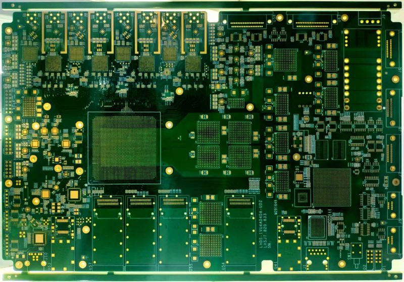
A PCB printed circuit board is a flat board that holds the electrical components of a device and connects them with copper traces. The traces on a PCB allow for electrical signals and power to be distributed to each component. The importance of a PCB lies in its ability to ensure the correct functioning of electronic devices by providing an efficient path for electricity.
What’s the real story? Without PCBs, modern electronics would not be what they are today. Whether it’s a smartphone, computer, or microwave, PCBs are present in almost every electronic device, ensuring proper functionality, reliability, and efficiency.
| Feature | Description |
|---|---|
| Substrate Material | The foundation of the PCB (usually fiberglass or composite material) |
| Copper Traces | Conductive pathways that connect electronic components |
| Solder Mask | Protective layer that prevents short circuits and protects the copper traces |
| Components | Includes resistors, capacitors, and other elements attached to the PCB |
The structure of a PCB includes several layers that serve different functions, with the most common types being single-sided, double-sided, and multi-layer PCBs. At the core, PCBs consist of layers of conductive copper that are etched to form the pathways for electrical signals, and insulating layers that ensure the traces are electrically isolated from one another.
The substrate serves as the foundation of the PCB. The most commonly used material for PCBs is FR4 (fiberglass), which is strong and reliable. Other materials, such as aluminum for metal core PCBs or ceramic for high-temperature applications, may also be used. The choice of substrate material affects the overall performance, cost, and reliability of the PCB.
Copper traces are the electrical pathways through which signals and power flow. These traces are created by etching copper foil, which is attached to the substrate. This process ensures that only the required traces remain, with excess copper being removed to avoid unwanted electrical paths.
Ready for the good part? The precise design and etching of these traces are what make the PCB function as intended, supporting the functionality of every electronic component on the board.
| Layer | Description |
|---|---|
| Substrate | Provides the structural base and electrical insulation |
| Copper Traces | Creates the conductive paths that link components |
| Solder Mask | Protects the copper traces and prevents short circuits |
| Silkscreen | Provides component labels and additional markings |
There are several types of PCBs, each tailored to specific applications. The choice of PCB depends on the complexity of the circuit design, the number of components, and the type of device. The three most common types are single-sided, double-sided, and multi-layer PCBs.
Single-sided PCBs have a single layer of copper traces on one side of the substrate. Components are placed on the other side, making this the simplest and most cost-effective type of PCB. It is typically used in devices that don’t require complex circuitry, such as basic toys or simple electronic gadgets.
Double-sided PCBs feature copper traces on both sides of the substrate. These boards allow for more complex designs as components can be mounted on both sides, and traces can be routed between layers. They are commonly used in products like smartphones and printers.
Multi-layer PCBs are made by stacking multiple layers of substrate and copper traces. This type of PCB is used for more complex designs where space and signal integrity are critical, such as in high-performance computing, medical devices, and telecommunications equipment.
This is where it gets interesting… The complexity and cost of a PCB increase with the number of layers. Multi-layer boards are ideal for high-density designs that require efficient space usage and high performance.
| Type | Characteristics | Common Applications |
|---|---|---|
| Single-Sided PCB | One layer of copper traces, simple design | Basic electronic devices like toys and calculators |
| Double-Sided PCB | Two layers of copper traces, more complex design | Consumer electronics like smartphones and printers |
| Multi-Layer PCB | Multiple layers of traces for high-density designs | High-performance devices like computers and medical equipment |
The materials used in PCB manufacturing directly affect the performance, cost, and durability of the final product. The most important material choices are the substrate, copper for traces, and the solder mask.
The substrate material is the base of the PCB and plays a crucial role in determining its mechanical properties, thermal stability, and electrical performance. Common substrates include FR4, CEM1, and CEM3, each offering different trade-offs in terms of cost, reliability, and suitability for specific applications.
Copper is the primary conductive material used for PCB traces. The thickness of the copper layer influences the board’s ability to handle current. In some applications, high-performance copper alloys are used to provide better conductivity, especially in power electronics and high-speed circuits.
The solder mask is applied to protect the copper traces and prevent soldering errors. The silkscreen layer is used to print component identifiers, logos, and other markings on the PCB for assembly and maintenance.
What’s the real story? The combination of these materials ensures that PCBs not only meet the electrical requirements but also perform reliably under a range of environmental conditions.
| Material | Description | Use Case |
|---|---|---|
| FR4 | Fiberglass-based substrate, cost-effective | General-purpose PCBs, consumer electronics |
| CEM1 | Composite epoxy material, less common than FR4 | Simple electronic devices and low-cost applications |
| Copper | Conductive material used for traces | All types of PCBs for power distribution and signal routing |
PCBs serve as the foundation for connecting electronic components. They provide a physical and electrical framework that allows components like resistors, capacitors, and integrated circuits (ICs) to interact.
Copper traces on the PCB are used to connect components and route electrical signals. The design of these traces must ensure that power is distributed evenly across the board, and signal integrity is maintained. In multi-layer PCBs, traces are routed through different layers, allowing for more complex designs.
The placement of components on a PCB is critical for both functionality and manufacturability. Components need to be placed in such a way that minimizes the length of traces and avoids interference. The routing of traces also impacts the overall performance of the board, particularly in high-speed and high-power applications.
As components work, they generate heat. In PCBs, especially those in high-power applications, managing heat dissipation is crucial to ensure the longevity and reliability of the board. Effective routing and material choices play a key role in managing heat on a PCB.
This is where it gets interesting… The layout and routing of a PCB are what ultimately make the difference between a device that works reliably and one that fails under heavy use.
| Function | Description |
|---|---|
| Signal Routing | Carries electrical signals between components |
| Power Distribution | Ensures even power supply to all components |
| Heat Dissipation | Manages the thermal flow to prevent overheating |
PCB design is not just about connecting components. It involves careful consideration of electrical, thermal, and mechanical aspects to ensure the board performs optimally.
The electrical design of a PCB must take into account the current carrying capacity of traces, impedance matching, and signal integrity. For high-frequency or high-speed designs, special attention must be given to minimizing noise and signal degradation.
Heat management is critical in high-power designs. PCB designers need to consider the amount of heat generated by the components and how to dissipate it effectively. This may include using heat sinks, thermal vias, or even selecting materials with higher thermal conductivity.
Mechanical design involves determining the size, shape, and layer configuration of the PCB. This is especially important when designing for specific enclosures or for multi-layer PCBs that require careful stacking of layers to meet the design specifications.
But here’s the kicker… A well-designed PCB ensures that every component works efficiently and reliably, helping devices function as expected in both everyday and harsh conditions.
| Consideration | Impact | Solution |
|---|---|---|
| Electrical Design | Affects signal integrity and power distribution | Proper trace width, routing, and impedance |
| Thermal Management | Ensures the board can handle heat generated by components | Use heat sinks, copper pours, and thermal vias |
| Mechanical Design | Determines the physical dimensions and layout | Use design software and ensure compatibility with the device |
The manufacturing process of a PCB involves several critical steps, from material selection to the final assembly. The steps ensure the integrity of the design and guarantee that the PCB meets the necessary standards for performance.
The first step in manufacturing a PCB is selecting the right materials. This includes choosing the substrate material, copper foil, solder mask, and silkscreen. Each of these materials must meet the specific requirements of the design, whether it’s for cost, performance, or durability.
In this step, the copper foil is etched to form the traces that will connect the components. The etching process is followed by drilling holes for vias, through-hole components, and mounting holes. Precision is key in this stage to ensure that the holes align with the components.
After etching and drilling, components are mounted onto the board. The most common methods are surface mount technology (SMT) and through-hole soldering. SMT is widely used in modern electronics for its ability to handle smaller components and higher-density designs.
What’s the real story? The manufacturing process requires careful control and precision to ensure that the finished PCB performs to specification.
| Step | Description | Importance |
|---|---|---|
| Material Selection | Choosing substrates, copper foil, solder mask, etc. | Determines performance and reliability |
| Etching and Drilling | Creating traces and holes in the PCB | Ensures electrical connections and component mounting |
| Soldering and Assembly | Mounting components and creating electrical connections | Finalizes the PCB design for use in devices |
Testing and quality control are essential in ensuring that the PCB meets the design requirements and will function reliably. Testing is performed at several stages throughout the manufacturing process.
Electrical tests ensure that the PCB functions as intended by checking for continuity, signal integrity, and power distribution. This can be done through automated testing equipment or manual inspection.
Mechanical testing checks the physical properties of the PCB, such as its durability, flexibility, and resistance to environmental stress. Thermal cycling, vibration testing, and other mechanical tests ensure that the PCB can withstand harsh operating conditions.
But here’s the kicker… Rigorous testing and quality control at each stage help prevent failures and ensure that the final product meets the required standards for performance and reliability.
| Testing Type | Description | Purpose |
|---|---|---|
| Electrical Testing | Checks for electrical faults like open circuits and shorts | Ensures proper functionality |
| Mechanical Testing | Tests physical durability and stress resistance | Ensures longevity in harsh environments |
PCBs are used in a wide range of electronic devices across various industries. From consumer electronics to medical devices, PCBs play a crucial role in ensuring the reliability and functionality of modern technology.
PCBs are widely used in smartphones, televisions, gaming consoles, and other consumer devices. These boards must be designed to handle a variety of components, from processors to sensors.
In the automotive and industrial sectors, PCBs are used in control systems, sensors, and power management systems. These applications require PCBs that can handle harsh conditions such as temperature extremes, vibrations, and exposure to chemicals.
PCBs in medical devices need to meet stringent reliability and safety standards. These devices often require PCBs that can function in demanding environments, such as inside the human body or in critical care equipment.
This is where it gets interesting… The diverse range of applications for PCBs highlights their importance in powering the devices that drive modern technology.
| Industry | Application | Requirements |
|---|---|---|
| Consumer Electronics | Smartphones, TVs, gaming devices | Small, reliable, and cost-effective designs |
| Automotive | Sensors, control systems, power management | Durable, heat-resistant, and high-performance |
| Medical Devices | Diagnostic tools, pacemakers | Precision, reliability, and safety standards |
In conclusion, PCBs are integral to modern electronics, connecting components and enabling devices to perform as expected. From basic circuits to complex multi-layer designs, PCBs are essential for ensuring the functionality, reliability, and longevity of electronic devices.
And now you know the full story on PCBs! By understanding their structure, materials, design considerations, and applications, you can optimize your PCB designs and contribute to the continued growth of electronics technology.
Q1: What is a PCB printed circuit board?
A1: A PCB is a flat board that connects electronic components using copper traces, providing the necessary electrical paths for signals and power.
Q2: How do PCBs work?
A2: PCBs work by using copper traces to connect various electronic components, allowing signals and power to flow through the circuit.
Q3: What are the different types of PCBs?
A3: The most common types of PCBs are single-sided, double-sided, and multi-layer boards, each serving different levels of complexity and functionality.
Q4: What materials are used in PCB manufacturing?
A4: Common materials for PCBs include FR4, copper for the traces, solder mask for protection, and silkscreen for component labeling.
Q5: How is a PCB tested for quality?
A5: PCBs undergo electrical and mechanical testing to ensure they meet performance standards and can withstand environmental conditions.


Connect to a Jerico Multilayer PCB engineer to support your project!
Request A Quote


 Quote
Quote