


+86 13603063656
Welcome to the definitive guide on the PCB process—your roadmap from digital design to finished board, packed with professional insights and industry best practices. Mastering the PCB process is not just about ticking boxes; it’s about understanding every detail that separates an average board from a reliable, high-performance product. This article walks through each crucial stage, highlights the must-know techniques, and unpacks how top manufacturers keep costs low without sacrificing quality. Ready for the good part? Let’s make your next PCB process your best yet.
PCB Process
The PCB process is the backbone of modern electronics manufacturing. But what’s the real story? Every smart device, control system, or industrial machine you use relies on a robust, repeatable PCB process. This process encompasses all stages: from electronic design to layout, through material selection, imaging, drilling, plating, and testing, right down to packaging and shipment. Why does this matter? Because mistakes at any step can cause failures, delays, or soaring costs for your business.
A well-controlled PCB process is a competitive advantage for any OEM, contract manufacturer, or tech startup. The right process boosts reliability, reduces waste, and supports rapid scaling.
| Stage | Key Output | Typical Responsibility |
|---|---|---|
| Design | Gerber/Drill/BOM files | OEM/Design house |
| Fabrication | Finished PCB | PCB manufacturer |
| Assembly | Populated PCB | EMS provider or OEM |
| Testing | QA-approved PCBA | Manufacturer/OEM |
| Packaging/Logistics | Ready-to-use boards | OEM/logistics |
Before the factory can do its magic, the process starts on the engineer’s screen. Ready for the good part? The accuracy of your PCB process depends on design data integrity. You’ll need industry-standard design tools (like Altium, Eagle, KiCAD, or Mentor), and you must generate clean Gerber files, well-documented drill files, and a complete BOM.
But here’s the kicker… Neglecting proper DFM (Design for Manufacturability) checks often results in costly redesigns and delays. Always run DRC (Design Rule Checks), validate against your fab’s capabilities, and specify any special needs up front.
| Essential File | Function | Common Format |
|---|---|---|
| Gerber | Copper/mask layers | RS-274X |
| Drill File | Hole locations/sizes | Excellon |
| BOM | Assembly info | CSV/Excel |
| Netlist | Connectivity check | IPC-D-356 |
| ReadMe | Special instructions | TXT/DOC |
Great designs start with clean, clear, and correct data.
What’s the real story about board materials? They’re not all created equal. The core of your PCB process relies on the correct choice of substrate. Most commercial boards use FR-4 for its cost and versatility, but applications with RF, heat, or mechanical stress may require Rogers, polyimide, aluminum, or special ceramics.
Here’s where it gets interesting… Each material affects your board’s performance, heat management, and cost. Working with reputable material suppliers can prevent hidden failures and long-term degradation.
| Material | Key Property | Typical Use |
|---|---|---|
| FR-4 | Cost-effective, stable | General electronics |
| Rogers | Low loss, high frequency | RF, telecom, radar |
| Polyimide | Flexibility, heat | Flex circuits, aerospace |
| Aluminum | High thermal conductivity | LEDs, power electronics |
Material choice isn’t just a technicality—it’s a competitive edge.
This is where your PCB process gets hands-on. Inner layer imaging is the step that defines where copper will remain or be removed. High-resolution photolithography exposes copper-clad laminates to UV through your design’s image, then a chemical etching process strips away unwanted copper.
But here’s the kicker… Defects at this stage, like under/over-etching, cause shorts, opens, or reduced current-carrying capacity. AOI (Automated Optical Inspection) is crucial to catch early mistakes.
| Step | Tool/Method | Risk if Skipped |
|---|---|---|
| Photoresist coating | Cleanroom, UV | Pattern inaccuracy |
| Exposure/development | Phototool, developer | Traces misaligned |
| Chemical etching | Acid bath | Copper left behind |
| AOI | Camera/computer vision | Undetected faults |
Consistent imaging and precise etching build the foundation for multilayer reliability.
Welcome to the heart of the multilayer PCB process—lamination. In this step, pre-etched inner layers are stacked with prepreg and copper foil, then pressed together under heat and pressure. This bonds everything into a solid, cohesive laminate.
But here’s the real story… Misalignment or uneven heat distribution can cause shorts, open circuits, or even delamination. Alignment pins, x-ray registration, and carefully monitored thermal cycles prevent costly failures.
| Lamination Parameter | Standard Value | Impact |
|---|---|---|
| Pressure | 150–200 psi | Layer adhesion |
| Temp | 170–200°C | Epoxy curing |
| Time | 1–2 hours | Outgassing, strength |
| Registration | <20 μm offset | Signal integrity |
Perfect lamination ensures robust, high-density multilayer builds.
Now, let’s punch some holes. Drilling is the next key phase in the PCB process—enabling electrical connection between layers. Mechanical drilling works for most vias, but high-density or microvias require laser drilling.
Here’s where it gets interesting… Every via type—through, blind, buried—has its own processing, cost, and reliability profile. Deburring and careful cleaning after drilling are essential, or you risk plating voids and electrical failures later.
| Via Type | Drilling Method | Application |
|---|---|---|
| Through | Mechanical | Standard multi-layer |
| Blind | Mechanical/Laser | HDI, compact layouts |
| Buried | Mechanical/Laser | Signal integrity, space |
| Microvia | Laser | Smartphones, HDI, IoT |
Precision here means signal continuity later.
Ready for the good part? Vias alone aren’t conductive until you add copper. Electroless copper deposition creates a thin, conductive seed layer over hole walls and inner copper. Electroplating thickens this up to the specified requirement, ensuring low resistance and mechanical strength.
But here’s the kicker… Plating thickness must be tightly controlled (typically 20–25 μm) to pass IPC standards. Poor plating leads to catastrophic via failures—so in-line thickness measurement and process audits are essential.
| Step | Description | Control Point |
|---|---|---|
| Cleaning | Desmear/conditioning | Hole wall prep |
| Electroless Copper | Chemical deposition | Seed layer quality |
| Electroplating | Current-driven copper add | Thickness, adhesion |
| QC/Test | Cross-section, resistance | IPC compliance |
Thick, uniform plating is the unsung hero of PCB reliability.
Outer layers are imaged and etched in a process similar to the inner layers, but now feature registration holes, finer traces, and more complex patterns for surface mount pads.
But what’s the real story? Outer layer defects are more visible and harder to fix—so AOI, registration control, and chemical balance matter more than ever.
| Feature | Typical Value | Process Consideration |
|---|---|---|
| Trace width | 75–250 μm | Signal integrity |
| Registration offset | <15 μm | BGA/HDI layout tolerance |
| Solder mask dams | 75–100 μm | Prevent solder bridging |
Get the outer layers right, and your assembly shop will thank you.
Solder mask keeps solder where it belongs and prevents shorts. Ready for the good part? The right mask process stops solder bridges and provides electrical insulation. Green is standard, but custom colors like black, blue, or white can support branding.
But here’s the kicker… Poor mask registration or incomplete cure leads to exposed copper and reliability issues. Screen printing is common, but spray coating or inkjet can improve registration for fine-pitch.
| Mask Type | Application Method | Best Use Case |
|---|---|---|
| Epoxy Liquid | Screen printing | Standard FR-4 |
| LPI | Spray/inkjet | HDI, fine-pitch |
| Dry Film | Lamination | Thick, high-end PCBs |
| Custom Color | Screen/spray | Branding, ID |
Mask choice is both an engineering and marketing decision.
What’s the real story with PCB finishes? Surface finish protects exposed copper pads and ensures reliable soldering. Your choices—HASL, ENIG, OSP, immersion tin or silver—each affect cost, assembly ease, and long-term reliability.
But here’s the kicker… The wrong finish can kill solderability or lead to early board failures. ENIG is preferred for fine-pitch and BGA; OSP is great for lead-free and green applications.
| Finish | Main Advantage | Limitation | Typical Use |
|---|---|---|---|
| HASL | Cost, availability | Not flat, RoHS? | General purpose |
| ENIG | Flat, long shelf life | Black pad risk, cost | BGA, HDI, medical |
| OSP | Green, low cost | Shorter shelf life | Consumer, lead-free |
| Immersion Silver | Flat, high quality | Tarnish, handling | RF, telecom |
Pick the right finish and watch your yield soar.
Let’s put your name on it. The silkscreen step prints component values, reference designators, and company logos onto the board.
Ready for the good part? Clear, accurate legends help avoid assembly mistakes, speed up troubleshooting, and protect your brand. Ink type, print resolution, and alignment are all critical—especially for high-density layouts.
| Parameter | Typical Value | Why It Matters |
|---|---|---|
| Ink type | Epoxy, UV curable | Durability, clarity |
| Color | White, yellow, black | Contrast, readability |
| Print method | Screen, inkjet | Resolution, alignment |
| Min text size | 0.8 mm | Avoids smudging |
Don’t let your silkscreen be the weak link in your PCB process.
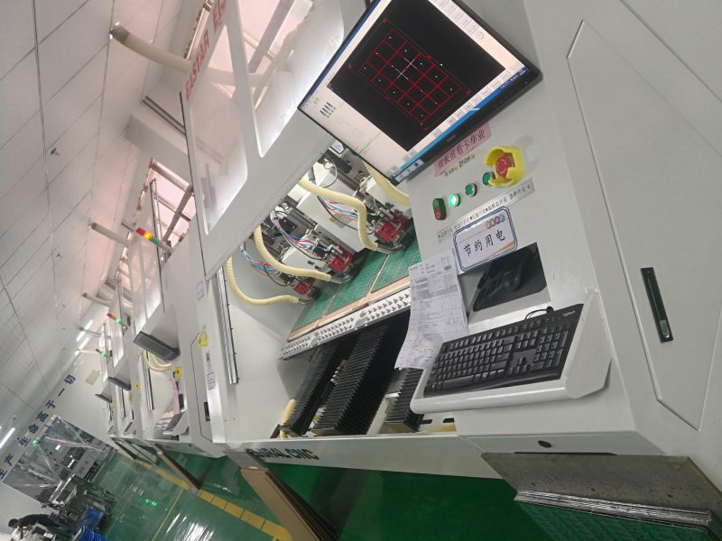
What’s the real story? The best PCB process in the world means nothing if the final product doesn’t work. Testing is your insurance policy. AOI (Automated Optical Inspection), flying probe, and bed-of-nails test systems detect open circuits, shorts, or misplaced traces.
But here’s the kicker… The more layers and complexity, the more essential testing becomes. X-ray inspection is often used for BGA, PoP, and dense via-in-pad designs.
| Test Method | Best For | What It Finds |
|---|---|---|
| AOI | All boards | Shorts, opens, solder mask |
| Flying Probe | Small batches, prototypes | Netlist errors, opens |
| Bed-of-Nails | High-volume | Shorts, full coverage |
| X-ray | HDI, BGA, hidden faults | Internal/via defects |
No board should leave the factory untested.
Time to cut things loose. After the panel is built, boards are routed, V-grooved, or tab-scored for separation.
But what’s the real story? Board separation is a mechanical process that must avoid chipping, rough edges, or mechanical stress. Tab routing is ideal for irregular shapes, while V-scoring is common for rectangular, mass-produced PCBs.
| Separation Method | Use Case | Note |
|---|---|---|
| Routing | Complex, curved boards | Custom profiles |
| V-scoring | Square, mass production | Faster depanelization |
| Tab-routing | Odd shapes | Manual break-off |
| Punching | Simple, thin boards | Limited precision |
Smart separation keeps yield up and post-processing to a minimum.
After all that, don’t let the last mile ruin your PCB process. Boards are cleaned to remove residues—ionic and organic contamination can cause corrosion and failures. ESD-safe packaging and humidity control prevent damage in transit.
Here’s the kicker… Mishandling at this stage can undo all the quality control before it. Use vacuum sealing, moisture indicators, and anti-static materials.
| Step | Method | Value Added |
|---|---|---|
| Cleaning | Ultrasonic, solvent, DI | Residue-free surfaces |
| Packaging | Vacuum, ESD, moisture | Prevents transit damage |
| Labeling | Barcodes, QR, ID labels | Traceability |
| Logistics | Courier, sea, air | Delivery flexibility |
Shipping is your first impression to the customer—make it count.
The story doesn’t end at shipment. Continuous improvement in the PCB process relies on robust quality assurance systems. Use IPC standards, lean manufacturing, SPC (Statistical Process Control), and Six Sigma tools to root out defects and boost yield.
But here’s the real story… Leading manufacturers close the loop with real-time monitoring, automated data capture, and regular process audits. This means lower defect rates and higher customer satisfaction.
| QA Practice | Tool/Standard | Benefit |
|---|---|---|
| IPC-A-600/610 | Visual, assembly checks | Standardized quality |
| SPC | Data/statistics | Ongoing process control |
| Six Sigma | DMAIC, PDCA | Yield, defect reduction |
| Traceability | Barcode/RFID | Root cause investigation |
Quality is never an accident—it’s engineered.
The PCB process is a sophisticated blend of science, technology, and craft. Mastering every step—from design and materials to testing and shipment—ensures your products stay ahead in quality, reliability, and performance. By working with skilled partners and never cutting corners, you can turn every order into a success story. Now, the next move is yours: build your next project on a solid PCB process foundation.
Q1: What is the PCB process?
The PCB process covers all steps from design to finished board production, including imaging, etching, plating, assembly prep, and testing.
Q2: How does multilayer PCB lamination work?
Layers are stacked, aligned, and bonded with heat and pressure, creating a single rigid unit with multiple interconnected layers.
Q3: What’s the role of surface finish in the PCB process?
Surface finishes protect copper, ensure solderability, and extend shelf life. Choice affects cost, reliability, and assembly quality.
Q4: Why is electrical testing crucial in PCB manufacturing?
Electrical testing ensures all circuits are connected as designed and detects open or short circuits before assembly.
Q5: How do manufacturers ensure quality during the PCB process?
They follow IPC standards, use advanced inspections, conduct process monitoring, and constantly optimize for fewer defects and higher yield.


Connect to a Jerico Multilayer PCB engineer to support your project!
Request A Quote


 Quote
Quote