


+86 13603063656
Printed circuit board (PCB) service is the backbone of modern electronics manufacturing, powering everything from IoT sensors to automotive systems. In today’s fast-paced B2B world, your choice of PCB service partner can make or break your product timeline, quality, and cost structure. But here’s the kicker… not all PCB service providers are created equal, and choosing wisely means understanding the full landscape—from design and prototyping through assembly and delivery. This comprehensive guide demystifies the PCB service journey, highlights the latest options, and gives you the tools to make informed, business-savvy decisions.

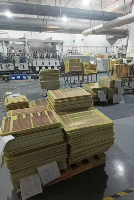
PCB Service
Let’s start with the basics: What is PCB service, and why should it matter to you?
PCB service refers to the full suite of professional offerings that help businesses turn an electronic schematic into a finished, functional printed circuit board. These services range from initial layout design, manufacturing and fabrication, and component sourcing, to assembly and testing.
But what’s the real story? For startups, having a reliable PCB service partner means you can launch products faster and with fewer headaches. For multinational manufacturers, the right provider brings consistency, technical support, and global logistics.
Consider three use cases:
| PCB Service User | Core Requirement | Best-fit Service Model |
|---|---|---|
| Startup | Fast prototyping, guidance | Turnkey, online platforms |
| Automotive Supplier | Quality, certification | Advanced fabrication, QA |
| Industrial OEM | Logistics, volume, flexibility | Integrated fab + assembly |
PCB service is a wide universe. Let’s break down the main types you’ll encounter.
There are three primary categories:
● PCB fabrication (the physical making of the board)
● PCB assembly (populating boards with components)
● Design, layout, and prototyping (turning ideas into manufacturable layouts)
But here’s the kicker… the best providers offer a seamless transition between all three, so you’re never left stuck at handoff points.
Three market scenarios:
| PCB Service Type | Typical Scope | When to Use |
|---|---|---|
| Fabrication Only | Bare board production | Rapid prototyping, cost control |
| Assembly Only | Soldering, mounting components | Custom builds, legacy products |
| Turnkey Service | Design to finished product | Startups, speed-critical projects |
So how does the journey really work? Let’s walk through it, step by step.
The PCB service process begins with initial design and file submission, followed by a sequence of engineering checks, fabrication, assembly, testing, and logistics. Every stage is an opportunity to avoid errors and ensure top quality.
Ready for the good part? Here’s a sample workflow:
| Stage | Key Activity | Critical Tools or Documents |
|---|---|---|
| Design | Schematic, layout | CAD, Gerber, BOM |
| Fabrication | Board production | CAM files, stackup drawing |
| Assembly | Parts mounting | Pick-and-Place, assembly plan |
| Testing | AOI, functional, ICT | Test points, X-ray |
| Logistics | Shipping, delivery | Barcode, packing list |
Fabrication is the art and science of creating the bare PCB. But here’s the real story… the difference between a robust, reliable board and a failure-prone one often comes down to fabrication quality.
What’s included in fabrication?
● Material selection (FR4, Rogers, aluminum, etc.)
● Copper weight, stackup design, via and trace definition
● Solder mask, legend, and surface finish (HASL, ENIG, OSP, etc.)
● Inspection and testing—AOI, flying probe, impedance test
Three fabrication case studies:
| Fabrication Feature | Options & Specs | When to Specify |
|---|---|---|
| Base Material | FR4, polyimide, metal | Thermal, RF, or flexible needs |
| Copper Thickness | 0.5–6 oz | Current handling, cost |
| Surface Finish | HASL, ENIG, OSP, gold | Solderability, shelf life |
| Certification | UL, ISO, IPC | Safety, export, auto/med markets |
Assembly is where bare boards become functional products. But here’s the kicker… the right assembly strategy can save weeks in development and thousands in warranty costs.
Assembly options:
● Surface Mount Technology (SMT) – ideal for volume and precision
● Through-Hole Technology (THT) – robust, good for high-reliability or power
● Mixed Assembly – combines both for complex layouts
Quality and inspection techniques include:
● Automated Optical Inspection (AOI)
● X-ray for BGAs and hidden joints
● Functional and in-circuit testing
Three assembly use cases:
| Assembly Method | Pros | Common Use Cases |
|---|---|---|
| SMT | Speed, miniaturization | Consumer, IoT, telecom |
| THT | Durability, strong joints | Power, auto, industrial |
| Mixed | Flexibility, complexity | Advanced controllers, medical |
This is where innovation starts.
Design and layout services help translate your circuit concept into a board that’s actually manufacturable. But here’s the real story… small mistakes here can cascade into expensive fab/assembly rework.
Key offerings:
● Schematic capture and PCB layout in Altium, Eagle, or KiCAD
● DFM and DFT consulting to prevent bottlenecks
● CAD-to-Gerber conversion, stackup optimization
Three design-driven scenarios:
| Design Service | Value Provided | Typical Client |
|---|---|---|
| Schematic Capture | Clean, error-free circuits | Startups, R&D teams |
| DFM/DFT Consulting | Manufacturability, testability | OEMs, complex boards |
| Layout Optimization | Signal, thermal, EMI | High-speed, high-reliability |
Speed is everything in today’s market.
Prototyping and quick-turn PCB service let you test, iterate, and improve before mass production. But here’s the kicker… fast isn’t useful if the results aren’t reliable.
Quick-turn options:
● 24–72 hour fabrication for single and multi-layer boards
● Rapid SMT assembly for pilot runs
● Engineering sample delivery with test reports
Three examples:
| Prototyping Service | Turnaround Time | Best-fit Customer |
|---|---|---|
| Fabrication only | 24–72 hours | R&D, proof of concept |
| Full assembly | 3–7 days | Pilot production, demo units |
| Quick-turn + DFM | 4–5 days | Short-run, high-complexity |
Let’s compare apples to apples.
A full turnkey PCB service manages the entire process—from parts sourcing to fabrication, assembly, and final QA. Partial turnkey means you (the client) provide some components or handle part of the workflow.
But what’s the real story? Full turnkey saves time and headaches, but may cost more. Partial gives you control over sourcing, but adds coordination risk.
Three business situations:
| Turnkey Model | Client Control Level | Pros | Cons |
|---|---|---|---|
| Full Turnkey | Low | Convenience, speed | Higher cost, less control |
| Partial Turnkey | Medium to high | Sourcing flexibility | More logistics, higher risk |
| Fab/Assembly only | Highest | Pure cost control | All sourcing responsibility |
The digital age has arrived in PCB service.
Online platforms provide instant quoting, file upload, tracking, and direct communication. But here’s where it gets interesting… platforms vary widely in support, capabilities, and logistics.
Popular features:
● Instant Gerber upload and DFM analysis
● Real-time pricing, shipping estimation, and order tracking
● Integration with BOM management and component sourcing
Three platform scenarios:
| Online Service | Core Advantage | Typical User |
|---|---|---|
| Instant quoting | Speed, transparency | Prototypers, startups |
| API integration | Batch management | Large OEMs, tech platforms |
| Live support | Problem-solving | First-time buyers, R&D |
Selecting a PCB service provider can be daunting. But here’s the kicker… focusing on the right factors saves money, reduces risk, and boosts product quality.
Top selection criteria:
● Certifications: ISO9001, UL, IPC, TS16949 (for auto), ISO13485 (for medical)
● Technical capabilities: Layer count, trace/space, min via size, assembly density
● Price, lead time, and MOQs
● Communication and support: Time zone, language, response speed
Three vetting cases:
| Criteria | Why It Matters | Typical Red Flags |
|---|---|---|
| Certification | Ensures safety, compliance | Missing, expired, irrelevant |
| Capability | Matches your technical needs | Limits on stackup, pitch |
| Service/Support | Smooth communication, fewer errors | Poor response, language gaps |
Here’s where details make or break your project.
Proper file preparation reduces delays, errors, and cost. But here’s the real story… file errors are the #1 cause of stalled projects and manufacturing defects.
Critical file types:
● Gerber files for all layers (copper, mask, silkscreen, outline)
● Bill of Materials (BOM) with MPNs, specs, and preferred brands
● Pick-and-Place and centroid files for assembly
● Assembly drawings, test instructions
Three documentation wins:
| File Type | Purpose | Common Issues |
|---|---|---|
| Gerber | Defines board layers | Missing, outdated |
| BOM | Component sourcing | Unclear specs, part conflicts |
| Pick & Place | Automated assembly | Wrong orientation, no fiducials |
It’s not all smooth sailing.
Using PCB services introduces potential pitfalls. But here’s the kicker… being prepared lets you solve most issues before they escalate.
Top challenges:
● DFM issues leading to production delays
● Lead time slippage from supply chain bottlenecks
● Language and communication barriers, especially with overseas suppliers
● Quality issues and disputes in board inspection or test results
Three challenge scenarios:
| Challenge | Common Cause | How to Mitigate |
|---|---|---|
| Lead time delay | Component shortage | Buffer stock, dual sourcing |
| Quality dispute | Inspection method mismatch | Agree on test plans upfront |
| Communication | Time zone, language | Use local support or agents |
PCBs power the modern world—here’s where service diversity matters.
Every industry has unique PCB service requirements. But here’s the real story… some sectors require ultra-robust boards, others demand speed and miniaturization.
Industry snapshots:
| Industry | Key PCB Service Requirement | Typical Application |
|---|---|---|
| Consumer/IoT | Speed, volume, miniaturization | Smartwatches, sensors |
| Automotive | Heat, vibration, traceability | ECUs, ADAS modules |
| Medical | Compliance, high reliability | Diagnostic, implantable devices |
| Industrial | Power, robustness | PLCs, drives, sensors |
| Aerospace | Reliability, specialty | Flight systems, satellites |
What’s the real story behind PCB service costs?
Cost drivers in PCB service include:
● Board size, layer count, and technology (HDI, rigid-flex, etc.)
● Surface finish, solder mask color, gold thickness, and other options
● Volume discounts, MOQ, and logistics costs
● Engineering or quick-turn surcharges
Three costing examples:
| Cost Driver | Low-Cost Option | High-Cost Option | Cost Impact |
|---|---|---|---|
| Board complexity | 2-layer, HASL | 8-layer, ENIG, HDI | 2–5x difference |
| Volume | 10 units | 10,000+ units | Up to 10x lower per unit |
| Assembly location | Offshore | Onshore/Local | 20–30% premium |
| Turnaround | Standard | 24–48hr quick turn | 2–4x higher |
So what’s the bottom line?
Maximizing value from your PCB service is about much more than just price. It’s about reliability, speed, support, and scalability. But here’s the kicker… the best PCB service providers aren’t just vendors—they’re partners in your business growth.
Key takeaways:
● Choose a provider with relevant certifications, proven technical capability, and solid reviews
● Communicate early and often—especially on file prep, test plans, and logistics
● Use rapid prototyping to shorten development cycles
● Consider full turnkey for speed, partial turnkey for cost or component control
Industry trends point toward more automation, AI-driven quoting, and tighter integration between fab, assembly, and logistics. Staying ahead means building long-term, strategic relationships with your PCB service partners.
| Key Value Area | How to Maximize Benefit |
|---|---|
| Speed | Use quick-turn + DFM partners |
| Quality | Specify certifications, test plans |
| Cost | Optimize for volume, local assembly |
| Support | Favor suppliers with real-time support |
real customer reviews.


Connect to a Jerico Multilayer PCB engineer to support your project!
Request A Quote


 Quote
Quote