


+86 13603063656
PCB silkscreen is a crucial aspect of printed circuit board (PCB) design, playing an important role in the functionality and aesthetic of electronic devices. In this article, we’ll delve into the significance of the silkscreen layer in PCB production, explore its manufacturing process, and provide tips for effective silkscreen design. The ultimate goal is to help you understand how PCB silkscreen contributes to the overall quality and usability of your products.
PCB Silkscreen
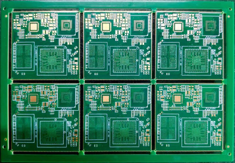
PCB silkscreen is the printed layer of ink on a PCB that displays symbols, labels, and logos to aid in component placement and product identification. This layer, usually applied after the solder mask and copper etching, is integral to the assembly and troubleshooting processes. Beyond merely serving a functional purpose, silkscreen provides visual clarity, helping manufacturers easily identify component locations and orientation. It’s crucial for clear markings on PCBs, particularly in complex designs with numerous components.
What’s the real story? Without proper silkscreen application, it would be significantly harder to identify components on the board, increasing assembly time and the potential for errors. Clear, well-designed silkscreen layers are essential for reducing mistakes during assembly and repair.
| Function | Description |
|---|---|
| Component Identification | Labels component positions for accurate assembly |
| Aesthetic Appeal | Enhances product look and branding |
| Aids in Troubleshooting | Helps engineers identify problems quickly |
The PCB silkscreen is applied using a printing process that involves transferring ink onto the surface of the PCB. This process ensures that critical component information, such as part numbers, polarity, and orientation, is clearly marked. The silkscreen layer is applied after the copper traces have been etched but before the soldering process begins.
The application of the silkscreen is typically done through screen printing, where a stencil is used to transfer ink onto the board. In some cases, a photolithographic process may be used for more intricate designs, especially in high-density applications. The ink used in the silkscreen layer needs to adhere well to the surface of the PCB and resist high temperatures during the soldering process.
Various types of inks are used, depending on the requirements of the PCB. The most common inks include epoxy-based, UV-curable, and inkjet-based formulations. These inks are chosen for their ability to withstand the temperatures and chemicals associated with the PCB manufacturing process.
Ready for the good part? The silkscreen is not just about function; it’s about providing clear, precise markings that aid in the ease of manufacturing and assembly.
| Ink Type | Features | Ideal Applications |
|---|---|---|
| Epoxy-Based | Durable, heat-resistant | High-temperature PCBs |
| UV-Curable | Cures quickly under UV light, resistant to fading | High-speed manufacturing |
| Inkjet-Based | Flexible, easy to apply in intricate designs | Low-volume or custom PCBs |
The choice of ink for PCB silkscreen is a crucial decision that directly impacts the board’s performance, longevity, and visual quality. Different inks are suitable for different applications based on the operating conditions and requirements.
Epoxy-based inks are known for their durability and heat resistance, making them a popular choice for high-temperature PCBs. These inks offer a strong bond and are less likely to peel off during the soldering process, ensuring that the silkscreen markings remain intact over time.
UV-curable inks are quick-drying and offer excellent durability once exposed to UV light. These inks are ideal for high-speed manufacturing, as they reduce curing times and increase production efficiency. Additionally, UV-curable inks are highly resistant to fading, ensuring that the markings remain visible for the life of the PCB.
For low-volume production or custom designs, inkjet-based inks are commonly used. These inks offer flexibility and are well-suited for intricate designs, although they may not have the same durability as epoxy or UV-curable inks. They are often used in prototyping or small batch production.
This is where it gets interesting… The choice of ink depends on the application’s specific needs, whether that’s durability, speed, or precision. Understanding the differences between ink types is key to achieving the desired outcome for your PCB design.
| Ink Type | Durability | Curing Method | Ideal Use Case |
|---|---|---|---|
| Epoxy-Based | High | Heat curing | High-temperature, industrial PCBs |
| UV-Curable | Very High | UV light curing | Fast manufacturing, high-volume production |
| Inkjet-Based | Moderate | Air drying | Custom, low-volume, or prototyping |
Designing an effective PCB silkscreen requires a balance between aesthetics, functionality, and legibility. The silkscreen is not just about placing labels; it’s about ensuring the board is easy to assemble, test, and maintain. Here are the key factors to consider when designing the silkscreen for your PCB.
The placement of labels and symbols should be clear and concise. Avoid overcrowding the board with excessive text or unnecessary markings. It’s essential to place text near relevant components to make identification easy during assembly. Consider the layout carefully, as it can impact both the functionality of the board and the ease of use for engineers and technicians.
Font size and type are crucial for readability. Use legible fonts that are easy to read even at smaller sizes. Common choices include sans-serif fonts like Arial or Helvetica, which provide clarity without being too ornate. Ensure the text is large enough to be visible during assembly and troubleshooting.
Clarity in silkscreen design is key. Misleading or unclear labels can lead to errors during assembly, which could compromise the PCB’s performance or cause failures in the final product. It’s essential to follow best practices for labeling components and keeping the design organized.
But here’s the kicker… When done right, the silkscreen layer can dramatically enhance the functionality of your PCB by making it easier to assemble, test, and troubleshoot. It’s not just about looks; it’s about improving the workflow.
| Design Element | Consideration | Best Practice |
|---|---|---|
| Text Placement | Keep labels near components for easy identification | Position labels according to assembly flow |
| Font Size and Type | Use clear, legible fonts | Choose sans-serif fonts in appropriate sizes |
| Marking Clarity | Ensure legibility of symbols and text | Avoid overcrowding the silkscreen area |
The PCB silkscreen layer offers a wide range of benefits that impact both the functionality and aesthetics of the board. This layer plays a crucial role in the overall performance of the PCB, especially during the assembly and troubleshooting processes.
By providing clear labels for each component, the silkscreen makes it easier to identify and install parts. Whether you’re building the board by hand or using automated systems, clear labeling is crucial to minimizing errors.
The silkscreen layer provides critical visual guidance during both the assembly and testing phases. Markings on the PCB help engineers and technicians identify component placements, orientations, and other critical details. This reduces assembly time and ensures that each component is correctly installed.
With clear silkscreen markings, the risk of assembly errors decreases, improving the overall quality of the finished product. Additionally, consistent silkscreen printing helps maintain uniformity across mass-produced PCBs, ensuring reliability and performance.
Ready for the good part? The benefits of a well-designed silkscreen go beyond just appearance—they’re crucial to improving the efficiency and reliability of the manufacturing process.
| Benefit | Description |
|---|---|
| Improved Readability | Clear labels make the board easier to assemble |
| Aids Assembly and Testing | Provides guidance during assembly and testing |
| Enhances Product Quality | Reduces errors and increases reliability |
Despite its importance, many PCB designs suffer from poorly executed silkscreens. These mistakes can lead to assembly issues, troubleshooting difficulties, and ultimately, reduced product quality. Let’s look at some of the most common mistakes in PCB silkscreen design and how to avoid them.
One of the most common mistakes is overcrowding the silkscreen with too much text or too many markings. This makes it difficult to read and can lead to confusion during assembly. It’s important to prioritize clarity over excessive labeling.
Not all inks are suitable for every PCB application. Using inks that aren’t compatible with the board’s environment or that can’t withstand high temperatures can cause silkscreen markings to fade or peel off over time. Always choose the right ink for your specific PCB application.
Misalignment during the silkscreen application process can lead to inaccurate markings, making it difficult to assemble the board correctly. Ensure precise alignment and proper calibration of printing equipment to avoid these issues.
This is where it gets interesting… Avoiding these mistakes can drastically improve the quality of the PCB and reduce errors during the assembly process.
| Mistake | Impact | Solution |
|---|---|---|
| Overcrowding the Silkscreen | Hard to read, confusing during assembly | Keep labels concise and well-organized |
| Using Incompatible Inks | Fading or peeling of silkscreen marks | Choose suitable, durable inks |
| Poor Alignment | Inaccurate markings, difficulty during assembly | Ensure proper alignment during printing |
While both the silkscreen layer and the solder mask are essential for the performance of a PCB, they serve very different purposes. The solder mask is designed to prevent oxidation and solder bridges, while the silkscreen layer serves to identify components and guide assembly.
The solder mask is typically a protective layer that covers the PCB, preventing solder from touching unintended areas during the soldering process. The silkscreen layer, on the other hand, is used for visual purposes, including component identification, polarity indicators, and other useful markings.
While the solder mask ensures electrical integrity and protection, the silkscreen layer improves the efficiency and accuracy of assembly. Together, these layers ensure that the PCB functions correctly and is easy to assemble and test.
What’s the real story? Without the combination of both layers, your PCB would be vulnerable to both assembly errors and environmental damage.
| Layer Type | Function | Role in PCB Design |
|---|---|---|
| Solder Mask | Prevents oxidation and solder bridging | Protects copper traces and pads |
| Silkscreen | Identifies components, labels parts, and orientation | Aids in assembly, testing, and maintenance |
Selecting the appropriate silkscreen for your PCB involves several considerations, including the type of PCB, the intended application, and the required durability. Choosing the right ink, design, and printing process is crucial for ensuring the success of your PCB.
When selecting materials, consider the temperature and chemical resistance of the inks. Ensure that the ink you choose will endure the heat of soldering and the environmental conditions the PCB will face during its lifespan.
Selecting the right ink type involves evaluating the manufacturing process, the board’s use case, and the desired durability. UV-curable inks may be suitable for high-speed production, while epoxy-based inks are better for high-temperature applications.
Ready for the good part? Choosing the right silkscreen material is essential for ensuring that your PCB is both reliable and easy to assemble.
| Consideration | Recommended Material Type | Ideal Application |
|---|---|---|
| High-Temperature Resistance | Epoxy-Based | High-temperature PCBs |
| Fast Manufacturing | UV-Curable | Mass production |
| Custom Design Needs | Inkjet-Based | Low-volume, custom PCBs |
High-volume PCB production presents unique challenges for silkscreen printing, particularly regarding speed, accuracy, and consistency. Ensuring quality across a large number of PCBs is essential for maintaining the integrity of the product.
In high-volume production, the primary challenge is maintaining consistency in the silkscreen layer across all boards. Small discrepancies in printing alignment or ink application can lead to defects, affecting the final product’s functionality.
One of the benefits of using silkscreen in high-volume production is the cost-effectiveness. Once the setup is done, printing becomes relatively inexpensive, and it can be done at high speeds.
This is where it gets interesting… The ability to maintain consistent silkscreen quality in large batches ensures that all produced PCBs meet the required standards and perform optimally.
| Consideration | Impact | Solution |
|---|---|---|
| Consistency | Inconsistent printing can lead to defects | Use automated alignment and calibration |
| Speed | Faster production times reduce costs | Implement high-speed printing systems |
| Cost-Effectiveness | High-volume production reduces per-unit cost | Optimize production workflow for efficiency |
PCB silkscreens are used across a variety of industries, with each sector requiring specific design considerations. From consumer electronics to high-reliability applications in medical and automotive fields, the silkscreen layer provides critical functionality and brand identification.
In consumer electronics, such as smartphones, gaming consoles, and laptops, the silkscreen layer is essential for component identification and assembly. Clear labeling ensures accurate placement of components, speeding up assembly and reducing errors. Additionally, it adds aesthetic appeal, enhancing the product’s look.
In automotive and industrial applications, PCBs are used in critical systems where reliability is paramount. Silkscreen layers not only help in the assembly process but also serve as a safeguard for maintenance by marking key components and their orientations.
Medical devices often involve complex PCBs that need to meet high standards of quality and reliability. The silkscreen layer plays an essential role in ensuring accurate assembly, which is crucial for devices that may have life-saving applications. In such industries, silkscreen marks are often more detailed, ensuring that components are correctly oriented and assembled.
What’s the real story? In high-reliability industries like medical and automotive sectors, the silkscreen layer’s accuracy and clarity are vital to ensuring product safety and performance.
| Industry | Application | Key Requirements |
|---|---|---|
| Consumer Electronics | Smartphones, gaming consoles, laptops | Accurate component placement, branding |
| Automotive | Engine control units, infotainment systems | Reliability, precise markings |
| Medical Devices | Diagnostic tools, monitoring equipment | High precision, clear identification |
As the electronics industry continues to focus on sustainability, the environmental impact of PCB manufacturing, including the use of silkscreen inks, has come under scrutiny. Eco-friendly alternatives are now available, helping manufacturers reduce their environmental footprint.
There has been an increasing push for environmentally friendly inks that are free from hazardous substances like lead and cadmium. Water-based inks and UV-curable inks are among the most popular eco-friendly options, as they contain fewer volatile organic compounds (VOCs) and are safer to use.
The Restriction of Hazardous Substances (RoHS) directive restricts the use of certain hazardous materials in electrical and electronic products. PCB silkscreen inks must comply with these regulations, ensuring that no harmful substances are used in the manufacturing process.
This is where it gets interesting… The growing trend of using eco-friendly materials in PCB manufacturing is not only better for the environment but also helps companies comply with global regulatory standards.
| Ink Type | Environmental Impact | Benefits |
|---|---|---|
| Water-Based | Contains fewer VOCs, safe to use | Safer for workers, easier to clean |
| UV-Curable | Cures under UV light, no solvents required | Reduces emissions, faster curing times |
| Soy-Based | Made from renewable resources | Non-toxic, biodegradable |
Despite the essential role of silkscreen in PCB production, issues can arise during the application process. From poor alignment to smearing and fading, troubleshooting silkscreen issues is vital to maintaining product quality.
One of the most common defects is poor alignment, where the silkscreen layer doesn’t line up correctly with the PCB’s components. Other issues include smearing, fading, and incomplete coverage, which can result from using incompatible inks or improper curing processes.
To address these defects, manufacturers should ensure that the silkscreen application process is carried out in a controlled environment. Regular calibration of printing equipment, along with using high-quality inks, can prevent most of these issues from occurring.
But here’s the kicker… Fixing these silkscreen issues early in the manufacturing process can save time and costs down the line, ensuring the quality of the final product is not compromised.
| Issue | Cause | Solution |
|---|---|---|
| Poor Alignment | Misalignment of printing equipment | Regular calibration and adjustments |
| Smearing or Fading | Incompatible inks or improper curing | Use suitable inks, ensure proper curing |
| Incomplete Coverage | Inadequate ink application | Apply a uniform layer of ink during printing |
As PCB manufacturing technologies continue to evolve, new techniques for applying silkscreen are emerging. These advanced methods improve both the accuracy and speed of silkscreen printing, making them essential for high-end production.
One of the most innovative techniques involves using lasers to etch silkscreen designs onto the PCB. This method allows for highly detailed and precise markings, which are crucial for PCBs with intricate designs or very small components.
Special inks that can withstand extreme environments are now available, allowing manufacturers to produce PCBs for high-performance applications like aerospace or military systems. These inks are more resistant to temperature changes, humidity, and other environmental stressors.
This is where it gets interesting… The ability to incorporate laser-etched silkscreen designs and specialized inks opens up new possibilities for manufacturing advanced PCBs with unique requirements.
| Technique | Benefits | Ideal Applications |
|---|---|---|
| Laser-Etched Printing | High precision, detailed designs | High-density or miniature PCBs |
| Specialized Inks | Resistance to extreme conditions | Aerospace, military, and automotive PCBs |
Silkscreening is an essential but often overlooked part of the PCB production process. The cost of applying the silkscreen layer can vary depending on factors such as ink type, design complexity, and production volume. Understanding these costs is important for manufacturers who want to ensure both high-quality and cost-effective production.
The silkscreen layer adds a small but important cost to the overall price of a PCB. However, this cost is typically outweighed by the value it provides in terms of ease of assembly and product identification.
Compared to other PCB processes such as soldering and etching, silkscreen printing is relatively inexpensive. However, when high volumes are involved, the costs of silkscreening can add up. Manufacturers must strike a balance between cost and the benefits of a well-executed silkscreen layer.
What’s the real story? While the silkscreen layer is an additional cost, its value in improving manufacturing efficiency and product quality makes it a wise investment.
| Cost Factor | Description |
|---|---|
| Ink Type | Specialty inks can increase costs |
| Design Complexity | Intricate designs may require more time and effort |
| Production Volume | High volumes reduce per-unit cost |
In conclusion, the silkscreen layer is an integral part of PCB design, providing both functional and aesthetic value. It aids in the assembly process, ensures proper component placement, and enhances the product’s visual appeal. Understanding the role of PCB silkscreen and how to design it effectively can lead to higher quality, more reliable products. Investing in a high-quality silkscreen layer is crucial for manufacturers who want to improve product performance and reduce errors during assembly.
And now you know the full story on PCB silkscreen! From the ink type to the design considerations, every aspect of the silkscreen layer plays a crucial role in ensuring the success of your PCB.
Q1: What is PCB silkscreen?
A1: PCB silkscreen is a printed layer on a PCB that provides identifying markings, logos, and text to assist in component placement and assembly.
Q2: How does PCB silkscreen work?
A2: Silkscreen is applied to the PCB using various printing techniques. It provides visible indicators like part numbers, orientation, and symbols to guide assembly and troubleshooting.
Q3: What are the types of PCB silkscreen inks?
A3: The main types of silkscreen inks include epoxy-based, UV-curable, and inkjet-based inks, each suited for different applications and environmental conditions.
Q4: Why is PCB silkscreen important?
A4: PCB silkscreen provides clear labels and component markings, making assembly easier, reducing errors, and improving the overall quality and functionality of the PCB.
Q5: What are common mistakes in PCB silkscreen design?
A5: Common mistakes include overcrowding the silkscreen, using incompatible inks, and poor alignment. These issues can lead to assembly difficulties and reduce product quality.


Connect to a Jerico Multilayer PCB engineer to support your project!
Request A Quote


 Quote
Quote