


+86 13603063656
PCB stackup refers to the arrangement of layers in a printed circuit board (PCB), which plays a crucial role in determining the board’s overall performance. The way these layers are stacked affects everything from signal integrity and thermal management to the board’s overall functionality. In this article, we will explore what PCB stackup is, how to design it effectively, the different types of stackups, and the factors to consider in making the best decisions for your board’s performance and manufacturability.
PCB stackup
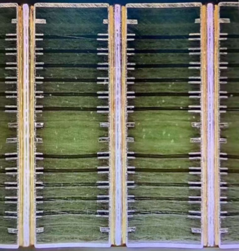
PCB stackup is one of the fundamental elements of circuit board design, referring to how various layers of the board are stacked together. These layers include the core, prepreg, copper, and soldermask, all of which are critical for the board’s electrical, mechanical, and thermal properties. But here’s the kicker: getting the stackup right is vital because it can influence everything from signal speed to heat dissipation. The stackup directly impacts the performance, manufacturability, and even the cost of the PCB.
The primary purpose of designing a PCB stackup is to provide an efficient and cost-effective layout that meets both performance requirements and the manufacturability standards of the PCB. Different applications, from consumer electronics to automotive systems, may require different stackup configurations based on factors like the complexity of the circuit and the need for high-speed or high-frequency performance. Understanding the types of stackups, materials used, and how to design an optimal stackup is essential for creating reliable and high-performance circuit boards.
| Factor | Description | Impact on Performance |
|---|---|---|
| Layer Types | Number and types of layers in the stackup | Determines overall board thickness and functionality |
| Material Selection | Choosing materials like FR4, copper, etc. | Affects durability, cost, and electrical performance |
| Trace Width & Spacing | Width of traces and spacing between them | Impacts impedance, signal integrity, and manufacturing ease |
PCB stackup refers to the specific configuration of the layers in a printed circuit board. Each layer serves a unique function: the core layer provides structural support, the copper layers are used for the electrical traces, and the prepreg layers act as insulation between copper and other layers. What’s the real story here? The arrangement of these layers determines the PCB’s electrical performance, signal integrity, heat management, and manufacturability.
A proper stackup design is crucial for ensuring that the electrical signals traveling through the PCB maintain their integrity. For high-frequency applications, stackup design is even more critical. For example, in high-speed circuits, signal traces must be carefully routed with controlled impedance to prevent signal degradation. Moreover, a well-designed stackup helps with minimizing crosstalk and reducing noise in the system. The complexity of a PCB stackup increases as the number of layers increases, especially when dealing with high-density designs.
| Layer | Description | Function |
|---|---|---|
| Core | A solid, thick layer of material (e.g., FR4) | Provides structural integrity |
| Prepreg | A resin-coated fiber material | Insulates and bonds other layers together |
| Copper Layers | Thin layers of copper foil | Forms electrical traces and pathways |
| Soldermask | A layer of green ink | Prevents solder bridges and protects traces |
| Silkscreen | A layer for printing text and symbols | Helps in component placement and identification |
PCB stackups come in different configurations, each designed to meet specific requirements for signal integrity, power distribution, and thermal management. The three main types of stackups are single-sided, double-sided, and multi-layer stackups. Let’s break it down further. Ready for the good part? The type of stackup you choose will impact everything from cost to performance.
Single-sided stackups are the simplest and most cost-effective, with copper traces placed only on one side of the board. Double-sided stackups offer copper traces on both sides of the PCB, doubling the available area for routing. Multi-layer stackups are the most complex, offering the highest performance but also requiring more advanced design and manufacturing processes. Multi-layer stackups are used in high-speed, high-frequency, and high-density designs.
The choice of stackup depends on the requirements of the specific application. For example, in consumer electronics, where cost is a major consideration, a double-sided stackup might be the ideal choice. For more advanced applications like high-frequency circuits, a multi-layer stackup with controlled impedance might be necessary.
| Stackup Type | Description | Best Use Case |
|---|---|---|
| Single-Sided | Copper traces on one side of the board | Low-cost, simple applications |
| Double-Sided | Copper traces on both sides of the PCB | Consumer electronics, low-frequency boards |
| Multi-Layer | Multiple copper layers interspersed with insulating layers | High-speed, high-density designs |
The materials used in PCB stackup design are just as important as the design itself. But here’s the kicker: using the right materials can make or break your PCB’s performance. The choice of materials, such as the base material (usually FR4), copper, and prepreg, affects electrical properties, heat dissipation, and overall board stability.
For example, FR4 is the most commonly used base material for PCB stackups, offering a good balance of strength, electrical performance, and cost. However, for high-frequency or high-speed applications, more specialized materials like Rogers or Teflon may be used for their lower dielectric constants, which help reduce signal loss. The prepreg material, which is made of resin and glass fibers, is also chosen based on the specific electrical properties required.
Another key factor is the thickness of the copper used in the stackup. Thicker copper layers are necessary for high-current applications but come at a higher cost. Material choices can also impact thermal management, as materials with high thermal conductivity, such as copper, are better suited for high-power applications.
| Material | Description | Best Use Case |
|---|---|---|
| FR4 | Glass-reinforced epoxy laminate | Standard consumer electronics and general PCB applications |
| Rogers | High-frequency PCB material with low loss | High-frequency, RF, and microwave circuits |
| Teflon | Low-dielectric material for high-speed applications | High-speed, high-frequency circuits |
| Copper | Metal used for traces and power distribution | High-power applications, thermal management |
Designing a PCB stackup requires careful planning to ensure that the board meets performance, cost, and manufacturing requirements. The first step is to determine the number of layers required based on the complexity of the design. But here’s the kicker: while more layers can improve performance, they also increase costs and manufacturing complexity. Balancing these factors is key to a successful PCB design.
Next, designers need to choose the right materials for each layer, considering factors like signal speed, power distribution, and thermal management. Layer order is also crucial—ground planes should typically be placed near the core to minimize noise, while power planes should be positioned to deliver stable power to the components.
Finally, it’s essential to consider trace width and spacing. High-speed designs require precise trace widths and spacing to ensure controlled impedance. Designers often use simulation tools to verify that the stackup meets the required electrical specifications before moving on to the physical manufacturing stage.
| Step | Description | Purpose |
|---|---|---|
| Layer Count | Determine the number of layers required | Optimizes the design for performance and cost |
| Material Selection | Choose materials for each layer | Ensures the stackup meets electrical, thermal, and mechanical needs |
| Layer Ordering | Arrange the layers, including power and ground planes | Optimizes signal integrity and minimizes noise |
| Trace Width & Spacing | Calculate the proper trace dimensions | Ensures impedance control and high-speed signal integrity |
Impedance control is one of the most crucial aspects of PCB stackup design, especially for high-speed and high-frequency circuits. What’s the real story? Impedance mismatch can lead to signal reflections, distortion, and loss of data, which is why managing impedance is essential for ensuring reliable performance.
Impedance control is achieved by carefully managing the width of traces and the distance between layers. For example, microstrip or stripline configurations are used to control impedance in high-speed designs. Designers must ensure that the impedance of signal traces matches the source and load impedances to prevent signal loss and degradation.
| Method | Description | Best Use Case |
|---|---|---|
| Microstrip | Signal trace runs on the outer layer of the PCB | High-speed, high-frequency applications |
| Stripline | Signal trace is sandwiched between layers | High-performance, multi-layer designs |
| Controlled Impedance | Designing the trace width and spacing to match impedance | RF, data transmission, and high-speed circuits |
Ground and power planes play a critical role in PCB stackup design. But here’s the kicker: these planes aren’t just there for electrical connections; they help reduce noise, maintain signal integrity, and improve thermal management. A well-designed power and ground plane configuration ensures stable power delivery to the components while reducing the risk of voltage drops and noise interference.
Power and ground planes should be placed close to each other in the stackup to provide a low-resistance path for the current. Additionally, using separate planes for power and ground can minimize the effects of electromagnetic interference (EMI) and crosstalk.
| Plane Type | Function | Design Consideration |
|---|---|---|
| Ground Plane | Provides a common reference for the circuit | Should be placed close to the core layer to reduce noise |
| Power Plane | Distributes power evenly across the PCB | Ensure sufficient decoupling and stable power delivery |
Signal integrity is a critical aspect of PCB design, and the stackup plays a major role in maintaining it. Poor stackup design can lead to issues like signal loss, crosstalk, and electromagnetic interference (EMI). Ready for the good part? By carefully designing the stackup and considering factors like trace width, layer spacing, and impedance control, engineers can ensure that signals remain clean and reliable as they pass through the board.
The key to maintaining signal integrity in high-speed designs is ensuring that the signal traces are routed in such a way that they avoid interference from other traces, power planes, or ground planes. Using ground planes to shield sensitive signals can also significantly improve performance.
| Factor | Description | Solution |
|---|---|---|
| Trace Routing | How traces are laid out on the PCB | Use proper spacing, controlled impedance |
| Layer Spacing | Distance between signal and reference planes | Maintain consistent layer distances for better shielding |
| Power/Signal Interference | Crosstalk between traces or noise from power planes | Use ground planes to shield signals |
Thermal management is a critical consideration when designing PCB stackups. High-power components generate heat, and without proper thermal management, the PCB can overheat, leading to component failure or reduced lifespan. But here’s the kicker: designing a stackup with thermal considerations helps dissipate heat more efficiently, ensuring that the components remain within their operational temperature range.
Thermal vias, copper pours, and thermal pads are commonly used in PCB stackups to enhance heat dissipation. Additionally, materials with high thermal conductivity, such as copper, are often used in high-power designs to help spread heat away from sensitive areas of the board.
| Strategy | Description | Best Use Case |
|---|---|---|
| Thermal Vias | Vias that help heat flow through multiple layers | High-power applications, LED circuits |
| Copper Pours | Large copper areas that act as heat sinks | Power distribution systems |
| High-Conductivity Materials | Materials that efficiently conduct heat away from components | High-performance, high-power circuits |
High-speed and high-frequency PCBs require careful stackup design to maintain signal integrity and avoid issues like signal degradation and crosstalk. The stackup must be designed to minimize the effects of electromagnetic interference (EMI) and ensure that signals are transmitted with minimal delay or distortion. Ready for the good part? High-speed designs often require advanced stackup configurations, such as using microstrip or stripline designs to control impedance and reduce signal loss.
When designing stackups for high-frequency circuits, it’s important to consider the placement of ground and power planes, the use of shielding, and the overall thickness of the PCB.
| Design Factor | Description | Best Practice |
|---|---|---|
| Impedance Control | Ensures consistent signal transmission | Use microstrip or stripline for controlled impedance |
| Ground and Power Planes | Properly placing planes to reduce noise | Keep ground planes close to signal layers |
| Shielding | Prevents external interference | Use copper pours and shields for sensitive traces |
While designing the perfect PCB stackup is essential for performance, it’s also important to understand the constraints imposed by the manufacturing process. But here’s the kicker: optimizing a stackup for manufacturability is just as important as designing it for performance. Manufacturers have limitations in terms of layer count, trace width, and spacing, and exceeding these limitations can increase production costs or result in manufacturing difficulties.
High layer count designs require more complex manufacturing processes, which can increase costs and lead to longer lead times. Additionally, certain materials may be more expensive or harder to work with, adding to the overall cost of production.
| Constraint | Description | Impact on Design |
|---|---|---|
| Layer Count | More layers increase complexity and cost | Higher cost and longer production time |
| Trace Width & Spacing | Smaller traces require higher precision | Difficult to achieve in high-layer designs |
| Material Availability | Not all materials are available in required quantities | Limited material options may increase costs |
Even experienced engineers can make mistakes when designing PCB stackups. Some common mistakes include improper layer ordering, incorrect trace width calculations, and failing to account for thermal or electrical requirements. What’s the real story? These mistakes can lead to poor PCB performance, increased costs, or even total circuit failure. It’s important to use simulation tools, follow industry standards, and carefully review the stackup design before moving forward.
Another common mistake is neglecting the impact of high-speed signals. In high-speed designs, improper impedance control or signal routing can cause significant signal integrity issues. Ensuring that the stackup is optimized for high-speed signals is crucial for achieving reliable performance.
| Mistake | Cause | Solution |
|---|---|---|
| Improper Layer Ordering | Layers not arranged correctly for optimal performance | Follow best practices for layer arrangement |
| Incorrect Trace Width | Trace dimensions not suitable for signal integrity | Use simulation tools to verify trace widths |
| Failing to Account for Heat | Not considering thermal management in high-power designs | Implement thermal vias and copper pours for heat dissipation |
In PCB stackup design, adhering to industry standards is crucial for ensuring quality and compliance. Standards like IPC-2221 and IPC-2222 guide the design and manufacturing processes, providing a framework for creating high-quality and reliable PCBs. But here’s the kicker: following these standards not only ensures that your PCB meets regulatory requirements but also improves manufacturability and performance.
The IPC standards, for example, cover everything from material selection and layer configuration to testing and inspection. They provide a comprehensive guide to designing PCBs that meet industry benchmarks for safety, performance, and reliability.
| Standard | Description | Coverage |
|---|---|---|
| IPC-2221 | Generic requirements for designing PCBs | Defines design requirements for manufacturability |
| IPC-2222 | Design and fabrication of multilayer PCBs | Guidelines for multi-layer PCB construction |
| IPC-2223 | Flexible circuit boards | Focuses on the design and manufacturing of flexible PCBs |
Designing PCB stackups requires specialized tools that help ensure precision and compliance with design requirements. Popular tools used for PCB stackup design include Altium Designer, Eagle, and KiCad. These tools offer features such as automatic impedance calculation, layer stack management, and simulation capabilities, which are essential for optimizing stackup designs. Ready for the good part? These tools not only streamline the design process but also help reduce errors and improve overall efficiency.
Using PCB design software also helps engineers visualize the final stackup before manufacturing, allowing them to identify potential issues and make adjustments early in the process.
| Tool | Features | Best Use Case |
|---|---|---|
| Altium Designer | Layer stack management, simulation tools | High-performance, complex PCB designs |
| Eagle | Affordable, user-friendly, with trace routing capabilities | Simple to medium-complexity PCBs |
| KiCad | Open-source, with layer stack and impedance control | Budget-friendly for hobbyists and smaller designs |
In conclusion, PCB stackup design is crucial for ensuring that the board performs optimally across various conditions. By selecting the right materials, controlling impedance, and considering factors like heat dissipation, manufacturers can create high-performance PCBs. The stackup configuration you choose will impact not only the performance but also the cost, manufacturability, and overall reliability of your design. With careful planning, simulation, and adherence to industry standards, optimizing the PCB stackup ensures a successful and reliable product.
Q1: What is PCB stackup?
PCB stackup refers to the arrangement of layers in a printed circuit board, including materials, copper layers, and insulating
layers, that affects the board’s performance.
Q2: How does impedance control work in PCB stackup?
Impedance control ensures consistent signal transmission through the PCB by managing trace width and layer spacing to match the required impedance.
Q3: What are the different types of PCB stackups?
PCB stackups include single-sided, double-sided, and multi-layer designs, each suited for different performance and cost requirements.
Q4: Why is thermal management important in PCB stackup design?
Thermal management in stackup design helps dissipate heat generated by high-power components, preventing damage and ensuring long-term reliability.
Q5: What are common mistakes in PCB stackup design?
Common mistakes include improper layer ordering, incorrect trace width calculations, and neglecting thermal or electrical performance requirements.


Connect to a Jerico Multilayer PCB engineer to support your project!
Request A Quote


 Quote
Quote