


+86 13603063656
PCB Tester: Complete Guide to Types, Methods & Best Practices. In modern electronics, the reliability of a printed circuit board (PCB) can make or break a project, brand reputation, or even a multimillion-dollar product launch. That’s why the role of a PCB tester is more vital than ever before. But what’s the real story? PCBs are the lifeblood of all electronic devices—from your coffee maker to a jetliner’s control system. The primary objective of this article is to provide a deep, yet accessible, exploration of PCB tester technologies, types, key functions, and their critical role in B2B electronics manufacturing. Whether you’re a procurement manager for an OEM, a manufacturing engineer, or a quality control leader, understanding PCB testers means controlling costs, reducing failures, and delighting customers. Ready for the good part? Let’s dive in and demystify the world of PCB testing from end to end.

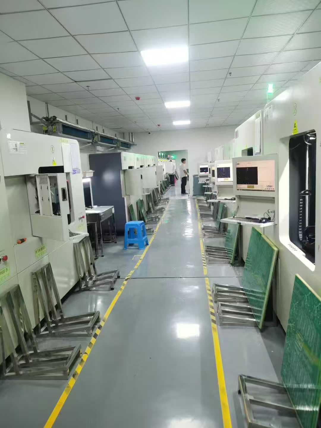
PCB Tester
PCB testers are not a one-size-fits-all tool—they come in a dazzling variety, each with its strengths and sweet spots. Here’s where it gets interesting: some testers are built for high-throughput mass production, while others shine in prototype or small-batch environments. The main categories are manual PCB testers, automated PCB testers, and specialized solutions such as in-circuit or flying probe testers.
Manual testers are as basic as it gets, relying on hand-held tools like multimeters and logic probes. They’re ideal for R&D labs, repair shops, and situations where flexibility and quick feedback matter most. Automated testers, on the other hand, include robust solutions like In-Circuit Test (ICT) machines, flying probe systems, and bed-of-nails fixtures. These deliver speed and repeatability at scale—essential for serious production environments.
But here’s the kicker: specialized testers now include ICT, flying probe, functional testers, and even optical inspection systems. Each has its use case, strengths, and limitations. For example, an ICT machine might test 1,000 boards per hour with 99.9% fault coverage but requires costly fixtures. Meanwhile, a flying probe tester excels for prototypes—no fixtures needed, quick setup, but slower on volume.
Check out the table summarizing the key types of PCB testers below.
| Tester Type | Main Use Cases | Pros | Cons |
|---|---|---|---|
| Manual | Repair, R&D, low volume | Flexible, low cost, hands-on | Slow, skill-dependent |
| ICT (Automated) | High volume, mass production | Fast, high coverage, repeatable | Expensive fixtures, setup time |
| Flying Probe | Prototyping, small runs | No fixture needed, flexible | Slower, less suited for high volume |
| Functional | End-product simulation/testing | Application-level testing, adaptable | Customization needed |
What’s under the hood of a PCB tester? At the core, these machines and tools are all about one thing: making sure every PCB leaves the line ready for action. But here’s the secret sauce—PCB testers perform a wide range of functions that extend far beyond a simple continuity check.
First up is continuity testing: ensuring that electrical paths are complete, and there are no unintended breaks. Next, shorts detection swoops in, hunting for those pesky unintended connections between traces that could spell disaster. Component verification is another critical function; testers confirm that every resistor, capacitor, or IC is not only present but installed in the right orientation and functioning within spec.
Let’s not forget test coverage—the more functions your PCB tester can perform, the higher your defect detection rate. A best-in-class tester can measure voltage, check impedance, perform boundary scans, and even analyze power-up sequences. That’s how modern electronics achieve their legendary reliability.
Let’s see these core functions summarized in the table below.
| Function | Purpose | Example Test | Failure Detected |
|---|---|---|---|
| Continuity | Ensure open circuits are closed | Trace check | Broken trace |
| Shorts Detection | Identify unwanted trace connections | Between nets | Solder bridge |
| Component Verification | Confirm values and presence | Resistor/IC check | Wrong part/missing part |
| Functional Testing | Simulate real-world operation | Power-on tests | Non-functioning PCB |
Let’s get straight to the point: PCB testing is not just a best practice—it’s a business necessity. But here’s the kicker: a single faulty PCB can cause a cascade of problems—product recalls, warranty claims, brand damage, or even safety risks. In B2B manufacturing, where reputation and reliability mean everything, robust testing is the backbone of operational excellence.
Testing ensures that every PCB rolling off the line meets rigorous quality and safety standards. Think about this: the global electronics industry loses billions annually to undetected PCB faults and field failures. That’s why leading brands invest heavily in advanced testers and meticulous QA protocols.
Still not convinced? Major electronics brands have slashed warranty costs and boosted customer satisfaction simply by tightening their PCB testing procedures. For example, a leading automotive supplier cut electrical failure rates by 80% after adopting automated ICT systems. What’s the real story? PCB testing transforms uncertainty into predictable quality—keeping your clients happy, your auditors satisfied, and your business competitive.
Here’s a look at the core reasons why PCB testing matters.
| Reason for Testing | Description | Business Impact |
|---|---|---|
| Quality assurance | Ensure defect-free products | Brand reputation, fewer returns |
| Compliance | Meet regulatory standards | Avoid fines, market access |
| Cost reduction | Fewer field failures and recalls | Higher margins, less rework |
| Customer satisfaction | Reliable, consistent products | Repeat business, positive reviews |
Sometimes, the tried-and-true manual methods are just what the doctor ordered. But don’t be fooled—manual PCB testing still plays a critical role, especially in design, repair, and low-volume production settings. What’s the real story? Skilled technicians use handheld multimeters for voltage, resistance, and continuity checks, often supplementing with logic probes to analyze digital signals.
Visual inspection is another vital step, leveraging magnifiers, microscopes, or the naked eye to spot solder bridges, missing parts, or poor joints. In small R&D teams or prototype builds, manual testing is fast, flexible, and can catch issues automated systems might miss—especially oddball design quirks.
Let’s look at some examples. In a prototype run for a wearable medical device, engineers discovered a misplaced resistor that automated testers had missed due to a software bug—manual visual inspection saved the day. In a PCB repair shop, a skilled technician found a cold solder joint by simply probing the suspect area while flexing the board.
Check the table for a breakdown of common manual testing methods.
| Manual Method | Key Tools Used | Best For | Limitations |
|---|---|---|---|
| Multimeter Checks | Multimeter | Continuity, voltage, current | Slow, skill-dependent |
| Visual Inspection | Magnifier, microscope | Solder joints, misplacements | Not quantitative, subjective |
| Logic Probes | Logic analyzer/probe | Digital signal verification | Requires experience |
Ready for the good part? Automated PCB testing is where manufacturing meets speed, precision, and scalability. In high-volume production, automated testers—especially In-Circuit Test (ICT), Flying Probe, and functional test setups—are the backbone of zero-defect manufacturing.
Automated testers can execute thousands of measurements per minute, quickly pinpointing faults that would take hours to catch manually. For example, a modern ICT system can check thousands of nodes for opens, shorts, and component values at breakneck speed. Flying probe testers use robotically controlled needles to test PCBs without requiring custom fixtures, making them ideal for prototypes and small batches.
What’s the real story? Automation doesn’t just speed up testing—it enhances traceability, enables data-driven improvement, and reduces human error. A major mobile phone OEM slashed defect rates by 75% after adopting automated flying probe testers on their prototype lines.
See the table below for an automated testing method comparison.
| Automated Method | Main Advantages | Best Applications | Key Limitation |
|---|---|---|---|
| ICT | Speed, coverage, reliability | Mass production | Fixture cost, setup time |
| Flying Probe | Flexible, no fixture needed | Prototyping, small runs | Slower than ICT |
| Functional Test | Simulates real-world operation | Final product QC | Custom setup, slower cycle |
Here’s where it gets interesting—in-circuit testing (ICT) is the gold standard for mass production. ICT uses a bed-of-nails fixture or pogo pins to make electrical contact with hundreds or thousands of test points on the PCB, allowing for simultaneous verification of circuit continuity, component presence, and correct orientation.
But what’s the real kicker? ICT offers lightning-fast throughput, with some systems testing up to 1,200 boards per hour and delivering 99%+ coverage on many designs. However, there’s a trade-off: ICT requires custom fixtures that are time-consuming and expensive to build. For high-mix or frequently changing designs, this can add significant cost and lead time.
Let’s consider a few case studies. In a consumer electronics factory, moving to ICT reduced time-to-market by two weeks and cut first-pass failure rates by over 60%. An automotive supplier saw ROI in under a year after automating 90% of their PCB testing via ICT.
Review the table for ICT essentials.
| ICT Attribute | Details | Significance |
|---|---|---|
| Fixture requirement | Custom bed-of-nails or probes | High setup cost, fast testing |
| Test coverage | 90–99% (varies by design) | High fault detection |
| Best use case | Large production runs | Scalable, repeatable |
| Cycle time | <1 minute per board | High throughput |
Let’s flip the script: flying probe testing is the agile alternative to ICT. Instead of requiring a costly, custom fixture, this method uses programmable robotic probes to move across the board, testing nets and components dynamically. Here’s the kicker—flying probe is perfect for prototypes, small batches, or fast-turn projects where flexibility is king.
Flying probe testers can test any board with minimal setup, adapt to design changes instantly, and still offer high fault coverage. The downside? Speed. They typically test fewer boards per hour than ICT systems, but their versatility and lower upfront costs are ideal for startups, R&D, or contract manufacturers handling lots of unique designs.
For example, a medical electronics OEM accelerated their prototype validation process by 40% using flying probe testers, while a contract manufacturer handling high-mix, low-volume runs saw a 50% reduction in fixture costs.
Let’s review flying probe tester features in this table.
| Feature | Advantage | Limitation |
|---|---|---|
| No fixture needed | Fast setup, low cost | Slower than ICT |
| Software-controlled | Flexible, easily reconfigured | May miss some component faults |
| High fault coverage | Catch open, shorts, polarity errors | Not ideal for mass production |
Now we get to the good part—functional testing is where the rubber meets the road. Instead of testing individual connections, this method powers up the assembled PCB and simulates its end-use environment. Think about it: functional testers check if the board does what it’s designed to do—run a motor, display graphics, process data—under real-world conditions.
Functional testing is essential for complex boards with processors, software, or custom peripherals. In B2B electronics, it’s often the final gatekeeper before shipping to a customer. Here’s the kicker: customized fixtures, software, and data logging are usually required, but the payoff is huge—catching any latent or intermittent faults before the product leaves the factory.
Examples? An industrial control manufacturer used functional testing to catch a rare microcontroller bug missed by ICT, saving $100,000 in potential field repairs. A smart device OEM leverages functional tests to validate firmware updates in production, slashing DOA (dead on arrival) units by 80%.
Here’s a table highlighting key aspects of functional PCB testing.
| Functional Test Aspect | Description | Benefit |
|---|---|---|
| Real-world simulation | Board powered, functions exercised | Catch subtle, system-level faults |
| Custom fixtures | Unique for each product | High fidelity, repeatable |
| Data logging | Automated test records/results | Traceability, analytics |
This is where it gets interesting—choosing the right PCB tester can make or break your production efficiency and product quality. But what’s the real story? You need to balance cost, speed, fault coverage, and adaptability.
Start with production volume: high volumes favor ICT; prototyping or low-mix favors flying probe or manual. Don’t forget about test coverage—the more critical the application (think medical, automotive, aerospace), the more comprehensive your testing must be. Budget and scalability are also key: investing in advanced automation makes sense for big runs but can be overkill for smaller jobs.
Let’s look at some examples. A wearable tech startup started with manual testing and migrated to flying probe as orders ramped up. A global automotive supplier deployed both ICT and functional testers to meet different quality gates for each product line.
The table below provides a cheat sheet for PCB tester selection.
| Need/Scenario | Best Tester Type | Why |
|---|---|---|
| High volume | ICT | Fast, repeatable, high coverage |
| Prototyping | Flying probe/manual | Flexible, low setup cost |
| Complex products | Functional testers | Application-level confidence |
| Budget constrained | Manual/flying probe | Lower upfront investment |
Integration is everything—your PCB tester isn’t just a standalone tool. It needs to fit seamlessly into the production line. Here’s the kicker: inline testers can be connected to conveyor systems for high-speed, automated quality gates. Offline testers are used for spot checks, troubleshooting, or batch sampling.
But there’s more—today’s best-in-class manufacturers use MES (Manufacturing Execution Systems) to track every board’s test results, giving full traceability from start to finish. Automated data upload and analytics let you spot trends, prevent future defects, and maintain compliance with ease.
A major electronics plant integrated inline ICT and functional testers, boosting throughput by 20% and virtually eliminating manual data entry errors. Another example: a small-batch EMS provider combined flying probe and manual test benches to stay flexible while meeting stringent customer requirements.
Here’s how production integration stacks up.
| Integration Approach | Benefit | Suitable For |
|---|---|---|
| Inline | Maximum speed, full automation | High-volume, low-mix |
| Offline | Flexibility, troubleshooting | R&D, prototyping, low volume |
| MES data integration | Full traceability, analytics | Regulated/critical industries |
Let’s dig into the nuts and bolts—what faults are PCB testers on the lookout for? Open circuits (broken connections) and shorts (unwanted connections) are the most common culprits. But here’s the kicker: sophisticated testers can also detect missing or wrong components, incorrect polarity, and even poor solder joints.
Soldering defects, like cold joints or bridges, often slip through visual checks but are caught by electrical testing. Testers also catch subtle issues like incorrect impedance or marginal component values—problems that could cause intermittent failures in the field.
Let’s consider three real-life examples. A power supply manufacturer traced a recurring field failure to a missing pull-down resistor, found only after targeted component verification tests. A telecom OEM detected an elusive open in a high-speed signal line using advanced impedance testing. Finally, a wearable device company found cold solder joints using automated AOI and continuity tests, reducing their return rate by 45%.
Review this table for common PCB tester fault detections.
| Fault Type | Test Method | Detection Impact |
|---|---|---|
| Open circuits | Continuity, flying probe | No power/functionality |
| Shorts | Shorts detection, ICT | Device failure, fire risk |
| Wrong/missing part | Component verification | Malfunction, erratic behavior |
| Soldering defects | AOI, continuity | Unreliable operation |
But what if a board fails testing? That’s where troubleshooting comes into play—a systematic approach using PCB testers to find and fix the root cause. Here’s the real story: start with high-level functional tests to see if the board powers up or runs its basic function. Then, narrow it down with continuity checks, shorts detection, and targeted component measurements.
In one memorable case, an industrial automation firm isolated a stubborn intermittent fault to a cracked via using a combination of flying probe and X-ray inspection. In another, a consumer electronics company relied on systematic troubleshooting to identify a faulty MCU socket causing production delays.
Best practices include documenting every step, using test data for failure analysis, and leveraging statistical process control to prevent future issues. Ready for the good part? Modern PCB testers can even store failure signatures and automate root cause suggestions, accelerating resolution.
Let’s summarize troubleshooting methods in the table.
| Troubleshooting Step | Tools/Methods Used | Value Added |
|---|---|---|
| Functional check | Power-on, system test | Confirms overall function |
| Continuity/shorts | Multimeter, flying probe | Pinpoints connection issues |
| Component analysis | ICT, probe, visual inspection | Identifies wrong/missing part |
| Advanced inspection | X-ray, AOI, signature analysis | Finds hidden/complex faults |
Ready for the kicker? Even the best PCB tester is only as good as its maintenance routine and calibration. Over time, test probes wear, fixtures degrade, and measurement accuracy can drift. Neglecting maintenance leads to false positives or missed defects—a costly mistake.
Regular maintenance should include cleaning, probe replacement, software updates, and calibration checks against traceable standards. A world-class PCB shop maintains a detailed log for every tester and sticks to a calibration schedule dictated by ISO or industry requirements.
For example, a telecom equipment supplier caught a major measurement drift in a functional tester during a routine calibration, avoiding costly rework on an entire production batch. Another firm extended the lifespan of their flying probe systems by following a strict cleaning and part replacement regimen.
Let’s highlight
key maintenance steps in the table below.
| Maintenance Activity | Frequency | Benefit |
|---|---|---|
| Cleaning/probe replace | Weekly/monthly | Consistent contact, fewer errors |
| Calibration | Quarterly/annually | Reliable measurements |
| Software updates | As released | Feature improvements, bug fixes |
| Log/records | Every event | Traceability, compliance |
What’s next for PCB testers? Buckle up, because innovation is moving fast. AI and machine learning are making inroads, with systems that learn from production data to predict and catch defects before they occur. Advanced diagnostics now use big data analytics to spot trends and optimize test coverage.
Miniaturization is another hot trend—testers are getting smaller, faster, and more integrated for use with micro-PCBs and densely packed electronics. Leading companies are also adopting cloud-based test result storage and sharing, improving collaboration across global teams.
Picture this: a future where self-learning testers reduce setup time to minutes and automatically generate optimized test plans. Or where mobile app-based testers allow engineers to diagnose faults from anywhere in the plant.
Here’s what’s on the horizon for PCB testing.
| Future Trend | Description | Expected Benefit |
|---|---|---|
| AI/machine learning | Automated test plan optimization | Fewer defects, higher yield |
| Advanced analytics | Data-driven diagnostics and improvement | Process insight, cost savings |
| Miniaturized testers | Suited for microelectronics, tight spaces | New applications, less footprint |
| Cloud integration | Centralized data, remote troubleshooting | Collaboration, faster fixes |
PCB Tester: Complete Guide to Types, Methods & Best Practices has walked you through the diverse, dynamic, and essential world of PCB testing. We’ve covered the main types, the core functions, the “why” behind rigorous testing, and best practices for choosing, using, and maintaining PCB testers. But here’s the real story: as electronics become more complex and quality demands rise, investing in the right PCB tester—and using it wisely—will remain a defining competitive edge. Stay current, stay sharp, and make every board count!
Q1: What is a PCB tester?
A PCB tester is a device or system used to check printed circuit boards for electrical functionality, defects, and component correctness before assembly or delivery.
Q2: How does a PCB tester work?
A PCB tester applies test signals and measurements to specific points on the board, verifying continuity, shorts, component presence, and proper operation through automated or manual methods.
Q3: What are the main types of PCB testers?
The main types include manual testers (multimeters, visual checks), automated in-circuit testers (ICT), flying probe testers, and functional testers for simulating real-world use.
Q4: How do you choose the best PCB tester for your needs?
Choose based on your production volume, test coverage requirements, budget, and whether you need flexibility for prototypes or speed for mass production.
Q5: What common faults can PCB testers detect?
PCB testers detect open circuits, shorts, missing or incorrect components, polarity issues, and soldering defects, ensuring only functional boards reach the customer.


Connect to a Jerico Multilayer PCB engineer to support your project!
Request A Quote


 Quote
Quote