


+86 13603063656
PCB vias are crucial for connecting different layers of a printed circuit board (PCB), allowing electrical signals to flow between them. The role of vias in PCB design cannot be overstated. Whether you’re designing simple single-layer boards or complex multi-layer boards, understanding PCB vias is essential for optimizing performance, reliability, and manufacturability. In this article, we will dive deep into the different types of PCB vias, their functions, and the best practices for incorporating them into your designs. Ready to enhance your PCB designs? Let’s get started!
PCB Via
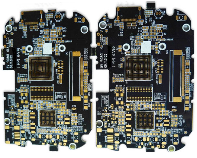
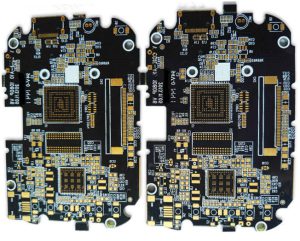
PCB vias are small pathways or holes that connect different layers of a printed circuit board (PCB). These vias serve as electrical bridges, allowing signals to pass between the layers, which is crucial for the functionality of multi-layer PCBs. Without vias, multi-layer PCB designs would be nearly impossible. The most common types of vias are through-hole, blind, and buried vias, each serving different purposes and suitable for different types of applications.
But here’s the kicker: understanding how each via type functions and the specific applications they’re best suited for can make or break a design. Properly chosen and placed vias can improve PCB performance, while improper use can lead to higher costs and potential failure of the board. Vias are indispensable in modern electronics, and mastering their use is key to successful PCB design.
Vias are created by drilling small holes through the PCB, which are then plated with copper to form a conductive path between the layers. The quality and precision of the via holes are critical for ensuring the integrity and performance of the PCB. The placement and design of vias must be carefully considered to maintain optimal signal integrity, minimize interference, and reduce the size of the board.
| Via Type | Layers Connected | Common Use | Pros | Cons |
|---|---|---|---|---|
| Through-Hole | Top to Bottom Layer | Standard designs | Simple, cost-effective | Takes up more board space |
| Blind | Outer Layers to Inner Layers | High-density boards | Efficient in dense designs | More expensive to produce |
| Buried | Inner Layers Only | Complex PCBs | Saves space, increases routing options | Higher manufacturing cost |
A PCB via is essentially a hole in the PCB that is plated with copper, creating a conductive path between layers. The via serves as a crucial connector that ensures signals travel between the different layers of a multi-layer PCB. Without vias, signal paths would be limited to a single layer, restricting the complexity and functionality of the PCB.
What’s the real story here? Vias are more than just a way to connect layers. They help manage the flow of electricity, minimize signal loss, and ensure the reliability of the entire circuit. Vias are critical in high-performance applications where space is limited, and there’s a need for complex routing. Vias allow designers to utilize more layers, creating a compact yet high-performance PCB.
There are different types of vias, each suited for different needs. Through-hole vias are the most basic and widely used type. They connect the top and bottom layers of a PCB. Blind vias connect the outer layers to the inner layers, while buried vias connect only the inner layers. Each type has distinct advantages depending on the design complexity and the number of layers involved.
| Via Type | Description | Ideal Use Case | Cost Consideration |
|---|---|---|---|
| Through-Hole | Passes through the entire PCB | Low-density designs | Low cost |
| Blind | Connects only outer to inner layers | High-density, compact designs | Moderate cost |
| Buried | Connects only inner layers | Complex, high-performance designs | High cost |
PCB vias play a pivotal role in connecting the various layers of a multi-layer PCB, making them indispensable for modern electronic devices. But here’s the kicker: the importance of vias extends far beyond just connecting layers. Vias impact the overall design of the PCB, from performance to cost, manufacturability, and even reliability.
Vias allow engineers to design more complex PCBs that are smaller and more compact. With vias, designers can fit more circuits into a smaller space, which is essential for creating the advanced electronic devices we rely on today. Whether it’s a smartphone, computer, or medical device, vias ensure that the circuits are connected correctly and function as intended.
Additionally, vias help manage the distribution of power and signals. They are crucial in preventing short circuits, ensuring that signals are routed efficiently, and maintaining the integrity of the PCB. Vias also play a role in heat management, as they help dissipate heat generated by high-power components. The failure of vias can lead to severe performance issues or even complete failure of the PCB, which is why careful design and testing are critical.
| Role | Impact on PCB Design | Example Applications |
|---|---|---|
| Electrical Connectivity | Allows signal flow between layers | Multi-layer boards in smartphones |
| Heat Dissipation | Helps distribute heat from power components | Power supplies, automotive electronics |
| Space Efficiency | Saves board space by enabling multi-layer designs | Consumer electronics, medical devices |
There are three main types of PCB vias: through-hole, blind, and buried. Each type has distinct characteristics and is suited for different types of PCB designs. Understanding these differences is key to selecting the right via type for your project.
Let’s break it down. Through-hole vias are the most basic type and are used to connect the top and bottom layers of a PCB. They are simple to manufacture and cost-effective but require more space on the PCB. Blind vias, on the other hand, connect the outer layers to the inner layers and are used in high-density designs where space is limited. They provide a more compact solution but are more expensive to produce.
Buried vias, the most complex type, are used to connect the internal layers of a PCB, with no direct connection to the outer layers. They are ideal for highly complex, high-density designs but come at a higher manufacturing cost. Each type of via serves a different purpose, and the choice depends on the specific design requirements and budget.
| Via Type | Layers Connected | Cost | Application Examples |
|---|---|---|---|
| Through-Hole | Top and Bottom | Low | Basic consumer electronics |
| Blind | Outer to Inner Layers | Moderate | High-density boards in smartphones |
| Buried | Inner Layers Only | High | Complex PCBs in aerospace or medical devices |
PCB vias work by creating a pathway for electrical signals to travel between different layers of the PCB. The process begins with drilling small holes through the PCB, followed by plating the holes with copper to create the electrical connections. These vias can be connected to different layers, allowing signals to pass through multiple layers and reach the appropriate components.
This is where it gets interesting… The manufacturing process behind vias can vary depending on the type of via and the complexity of the PCB. For through-hole vias, the holes are drilled through the entire PCB, while blind and buried vias require more advanced techniques like laser drilling. Each type of via must be carefully planned to ensure that the electrical connections are stable and reliable.
Vias also play an important role in the routing of power and ground planes. In multi-layer PCBs, vias are used to connect the power and ground layers, ensuring that the circuit functions properly. Proper via design helps to minimize the risk of signal interference, heat buildup, and electrical shorts.
| Step | Description | Importance |
|---|---|---|
| Drilling | Creating the hole in the PCB | Basic step for all vias |
| Plating | Adding copper to the drilled holes | Enables electrical connections |
| Testing | Ensuring via continuity and reliability | Ensures functionality and performance |
The design of PCB vias is crucial for ensuring the overall performance and reliability of the board. Several factors need to be considered when designing vias, including their size, placement, and routing. These factors can significantly impact signal integrity, thermal management, and manufacturability.
What’s the real story here? Via size plays a critical role in determining the performance of the PCB. Larger vias can handle more power and provide better heat dissipation, but they also take up more space. Smaller vias are ideal for high-density designs but can be more challenging to manufacture. The placement of vias is equally important, as improper via placement can lead to signal interference and heat buildup, negatively affecting PCB performance.
In high-performance applications, designers must also consider the type of via to use. Through-hole vias are simple and cost-effective, but they take up more space. Blind and buried vias are better suited for compact designs but require more advanced manufacturing techniques.
| Design Factor | Impact on PCB Design | Considerations |
|---|---|---|
| Via Size | Affects space and power handling | Larger vias are better for heat dissipation |
| Via Placement | Affects signal integrity | Proper placement reduces interference |
| Via Type | Affects complexity and cost | Blind and buried vias are for complex designs |
Multi-layer PCBs are commonly used in complex electronics, where space is limited, and high component density is required. Vias play a crucial role in multi-layer PCBs by connecting the layers, allowing signals to travel between different parts of the circuit. The design of the vias is crucial for ensuring the integrity of the PCB and its performance in high-density applications.
But here’s the kicker: multi-layer PCBs often use a combination of via types, such as through-hole and blind vias, to ensure the board’s compactness while maintaining high functionality. Vias in multi-layer designs help create efficient routing paths for electrical signals, reducing interference and improving overall performance. They also enable better power distribution and heat management, which is critical for high-performance applications.
| Via Type | Layers Connected | Application |
|---|---|---|
| Through-Hole | Top to Bottom Layer | Simple multi-layer designs |
| Blind Vias | Outer to Inner Layers | High-density designs |
| Buried Vias | Inner Layers Only | Complex multi-layer designs |
The size of a PCB via has a significant impact on its functionality, performance, and manufacturability. Larger vias can carry more power, but they also take up more space on the board. Smaller vias, while ideal for compact designs, have limitations in terms of current capacity and heat dissipation.
What’s the real story here? The size of the via should be chosen based on the requirements of the application. For example, in high-power applications, larger vias are needed to handle the increased current flow, while smaller vias are suitable for high-frequency circuits that require minimal interference. Choosing the right size is essential for ensuring both performance and cost-effectiveness.
| Via Size | Impact on Performance | Best Use Case |
|---|---|---|
| Larger Vias | Better power handling, heat dissipation | High-power circuits |
| Smaller Vias | More space-efficient, faster signals | High-density designs |
Via filling and plating are key processes in PCB manufacturing. Via filling involves filling the via hole with a conductive material, which ensures that the via functions properly as a connector between layers. Plating, on the other hand, involves coating the via with copper to create the electrical connection.
Ready for the good part? Via filling and plating are essential for high-performance applications, as they improve the electrical properties of the vias, making them more reliable and durable. Via filling is especially important in high-frequency designs, as it helps reduce signal loss and prevents unwanted electrical noise.
| Technique | Purpose | Application |
|---|---|---|
| Via Filling | Improves electrical connection | High-frequency PCBs |
| Via Plating | Creates conductive pathway | Multi-layer PCBs, high-performance circuits |
Via inspection is a critical step in PCB testing, ensuring that the vias are properly formed, plated, and functional. Inspection methods include visual checks, Automated Optical Inspection (AOI), and electrical testing. The goal is to detect any defects that may have occurred during the manufacturing process, such as incomplete plating or poor alignment.
But here’s the kicker: thorough via testing ensures that the PCB will perform reliably in its final application. Any defect in the vias could lead to a failure in signal transmission, power distribution, or overall functionality. Therefore, PCB manufacturers must prioritize via inspection to maintain high quality and reliability.
| Inspection Method | Purpose | Advantages |
|---|---|---|
| Visual Inspection | Check for visible defects | Quick and cost-effective |
| AOI | Automated defect detection | High accuracy, fast |
| Electrical Testing | Check for continuity and function | Ensures via reliability |
Advanced PCB via technologies, such as micro-vias and high-density interconnect (HDI) vias, are becoming more common as electronic devices continue to shrink in size and complexity. Micro-vias, which are tiny vias, allow for more compact designs, enabling higher component density without sacrificing performance.
What’s the real story here? These advanced via technologies allow for faster, more efficient circuit designs, but they also present new challenges in terms of manufacturing precision and cost. As the demand for smaller, faster, and more efficient electronics grows, these via technologies will continue to evolve to meet the needs of the industry.
| Technology | Feature | Use Case |
|---|---|---|
| Micro-Vias | Small, high-density vias | High-performance electronics |
| HDI Vias | High-density interconnect vias | Smartphones, wearable devices |
As PCBs become more complex, so do the challenges related to via design and manufacturing. Multi-layer PCBs, high-density designs, and micro-vias all require precise via placement and design to ensure proper functionality. The challenge lies in balancing the size and placement of vias with the need for electrical performance and manufacturability.
This is where it gets interesting… Designers must also consider the impact of vias on heat dissipation and signal integrity. Poor via design can lead to overheating, interference, and even total failure of the PCB. Advanced techniques such as via filling, plating, and optimized via placement can help mitigate these issues.
| Challenge | Impact | Solution |
|---|---|---|
| Small via size | Limits power handling | Use larger vias for power |
| Poor placement | Signal integrity issues | Proper via placement |
| Heat dissipation | Overheating and component failure | Use via filling, thermal pads |
Via design is one of the primary factors that affect the overall cost of PCB manufacturing. Simple via designs, such as through-hole vias, are relatively inexpensive to produce, but more complex via designs, such as micro-vias or buried vias, increase the cost due to the additional steps involved in manufacturing.
But here’s the kicker: while complex via designs increase the cost, they often lead to more compact, higher-performance PCBs, which are essential for today’s high-tech applications. Balancing via design with cost efficiency is a key part of the design process.
| Via Type | Cost Impact | Ideal Use Case |
|---|---|---|
| Through-Hole | Low cost, simple design | Basic consumer electronics |
| Blind and Buried | Moderate cost | High-density designs |
| Micro-Vias | High cost, advanced technology | High-performance electronics |
The future of PCB via technology looks promising as manufacturers continue to push the limits of miniaturization and performance. Emerging trends include the development of via-less PCBs and advanced via technologies that improve signal integrity, reduce size, and increase the efficiency of PCB designs.
What’s the real story here? Via technology will continue to evolve with the demands of next-generation electronics. Innovations like laser drilling, advanced plating techniques, and new materials are helping create faster, more efficient vias that will shape the future of PCB design.
| Trend | Description | Potential Impact |
|---|---|---|
| Via-less PCBs | Eliminates traditional vias | Compact, faster designs |
| Advanced Laser Drilling | Improves precision in via creation | High-density designs |
| New Plating Techniques | Reduces signal loss and increases reliability | Better performance |
PCB vias are critical components in the design and function of modern electronics. They enable multi-layer PCBs to connect electrical pathways across layers, allowing for more complex and compact circuit designs. By understanding the different types of vias, their applications, and the challenges associated with their use, PCB designers can create high-performance, reliable products. As technology continues to evolve, so too will the methods and technologies behind PCB vias, offering even more opportunities for innovation and advancement in the field.
Q1: What is a PCB via?
A PCB via is a hole in a printed circuit board that is plated with copper, creating a conductive path between layers, allowing signals to pass between them.
Q2: How do blind and buried vias differ from through-hole vias?
Blind vias connect the outer layers to inner layers, while buried vias connect only the inner layers. Through-hole vias pass through the entire PCB.
Q3: Why is via placement important in PCB design?
Proper via placement ensures that signals are routed efficiently, minimizing interference, and optimizing performance while maintaining board space.
Q4: How do vias impact signal integrity?
Vias can affect signal integrity by introducing impedance mismatches and noise. Proper design and placement are crucial for minimizing these effects.
Q5: What are micro-vias, and when should they be used?
Micro-vias are very small vias used in high-density PCBs. They are ideal for compact designs and high-performance electronics where space is limited.


Connect to a Jerico Multilayer PCB engineer to support your project!
Request A Quote


 Quote
Quote