+86 13603063656

xia@pcbsupplier.com

Sign in
X
2025-03-18 226
PCB Via Filling Guide: How to Choose the Best Via Filling Method?

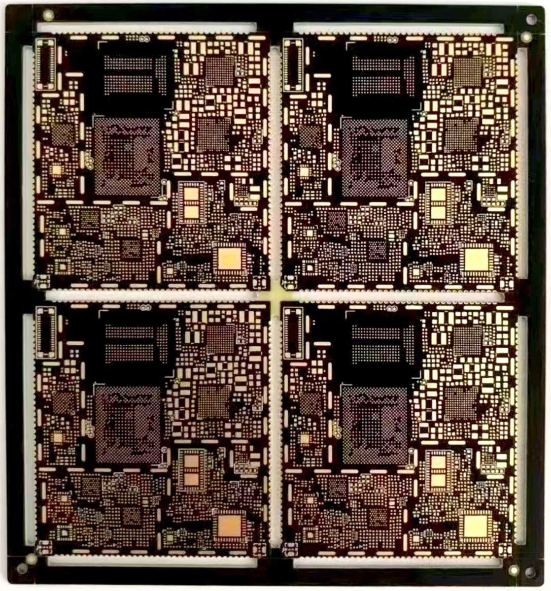
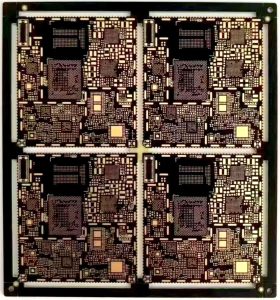
PCB Via Filling, In the PCB industry, via filling is not just a manufacturing step—it is a critical technology that determines the quality, performance, and reliability of a circuit board. Whether for high-speed signal transmission, thermal dissipation optimization, or multilayer board stability, via filling plays a vital role. However, engineers and procurement teams often struggle with several key questions when selecting a via filling method:

  • Non-conductive vs. conductive via filling—which is better for high-density PCBs?
  • How does the choice of via filling material affect signal integrity?
  • How to prevent electrical failures and mechanical defects caused by improper via filling?
  • How to balance cost and performance?

This guide will dive deep into different via filling technologies and help you make the best decision for your PCB projects.

PCB Via Filling

PCB Via Filling


What Is PCB Via Filling?

In PCB design, vias connect different circuit layers, and via filling refers to completely sealing these vias with filling materials to improve the board’s performance and durability. Depending on the application, filling materials can be resin, copper, epoxy, or solder mask, and different filling methods impact PCB functionality in distinct ways.

The Difference Between Via Filling and Via Plugging

Many people confuse via filling with via plugging, but they are fundamentally different:

  • Via filling: Completely fills the via, enhancing mechanical strength, heat dissipation, and electrical performance.
  • Via plugging: Only covers the via opening with solder mask or solder paste, mainly to prevent solder flow during assembly.

Understanding this distinction helps engineers avoid unnecessary design mistakes.


Common Applications of Via Filling in PCBs

Via filling is widely used in high-end electronics, particularly in the following applications:

  • High-speed, high-frequency circuit boards: Reduces signal interference and enhances EMC performance.
  • Multilayer PCBs: Improves structural stability and prevents interlayer short circuits.
  • Heat-sensitive circuits: Enhances thermal conductivity and extends component lifespan.
  • Automotive, aerospace, and 5G communication: Improves electrical performance and durability.

Different applications require different via filling methods, making the right selection crucial.


Types of Via Filling and Their Advantages & Disadvantages

Non-Conductive Via Filling (Solder Mask Over Via, Ink Plugging, and Resin Filling)

1. Solder Mask Over Via (SMOV)

  • Covers the via opening with solder mask without actually filling the hole.
  • Suitable for standard PCBs with no strict reliability requirements.

✅ Lowest cost
✅ Works for low-end consumer electronics
❌ Not suitable for BGA or high-density designs

2. Ink Plugging (Non-Conductive Ink-Filled Via)

  • Fills the via with solder mask ink, preventing solder wicking during assembly.
  • Widely used in automotive circuit boards and mainstream computer motherboards.

Sufficient for most PCB applications
Industry-standard for automotive and motherboard PCBs
Lower cost compared to resin-filled vias
❌ Lower mechanical strength than resin filling

3. Resin Filled Via (Non-Conductive Resin Filling)

  • Fills vias with epoxy resin and planarizes them, making it ideal for BGA and SMD applications.
  • Used in high-end HDI boards and multilayer PCBs to prevent solder overflow.

✅ Best mechanical strength
✅ Ideal for high-density interconnects and microvia filling
❌ Higher cost

📌 Cost Comparison (Based on Double-Layer & Four-Layer PCBs):

PCB Layer Count Solder Mask Over Via Ink Plugging Resin Filling
Double-layer PCB 1.00 1.02 2.00
Four-layer PCB 1.00 1.01 1.60

📢 In most cases, ink plugging is sufficient, especially for automotive electronics and mainstream motherboards, as it balances performance and cost effectively.


Conductive Resin Via-Filling

  • Description: Resin filled with conductive metal particles to enhance electrical conductivity and heat dissipation.
  • Best for: High-power circuits and low-impedance PCB applications.

✅ Improves electrical performance
✅ Ideal for high-frequency applications
❌ Higher cost and complex manufacturing process


Copper Filled Via

  • Description: Electroplated copper fills the via completely, forming a conductive bridge with extremely low resistance.
  • Best for: High-speed signal boards, RF circuits, and power electronics.

✅ Superior electrical performance
✅ Excellent heat dissipation
❌ High manufacturing cost


Key Factors to Consider When Choosing a Via-Filling Method

Electrical Performance vs. Mechanical Strength

  • High-speed signal boards should opt for copper-filled or conductive resin-filled vias to ensure signal integrity.
  • Multilayer PCBs require non-conductive via filling to prevent interlayer short circuits.

Thermal Dissipation Needs

  • High-power circuits should use copper-filled vias for optimal heat dissipation.
  • General applications can use non-conductive resin to reduce costs.

Cost vs. Manufacturing Feasibility

  • On a budget? Choose ink plugging, as it is sufficient for most applications.
  • For high-end PCBs? Opt for resin or copper-filled vias to optimize electrical and thermal performance.

How to Avoid Common Via-Filling Defects?

Common Issues & Solutions

🔴 Uneven filling → May cause short circuits or electrical failures.
🔴 Filling material expansion → Affects soldering reliability.
🔴 Trapped air pockets → Can interfere with signal integrity.

✔️ Select high-quality filling materials with good fluidity and adhesion.
✔️ Use vacuum filling processes to eliminate air pockets.
✔️ Perform strict AOI inspections to ensure via quality.

Also IPC  has the quality std in thid field


Conclusion: How to Make the Best Choice?

Selecting the right via-filling method depends on your PCB’s application, signal requirements, thermal demands, and budget.

  • Standard consumer electronics & automotive motherboards? Ink plugging is cost-effective and sufficient.
  • High-end BGA & multilayer HDI boards? Resin filling ensures mechanical strength and reliability.
  • High-power, high-frequency applications? Copper-filled vias provide the best conductivity and heat dissipation.

The right choice enhances PCB performance while optimizing manufacturing costs, ensuring long-term reliability in electronic products.

also anything you can communicated with your PCB supplier, they will rpely you the best choice

Connect to a Jerico Multilayer PCB engineer to support your project!

Request A Quote
Quote
E-mail Skype Whatsapp