


+86 13603063656
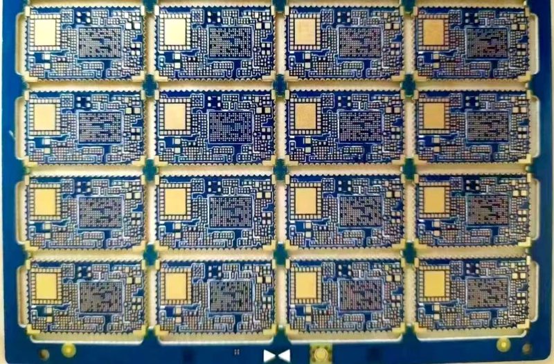
Printed circuit board printer. This tool changes everything for electronics professionals who need fast, in-house prototyping. Traditional PCB prototyping wastes time and exposes IP. But here’s the kicker… with a PCB printer, you can fabricate functional boards right at your desk, within hours.
A printed circuit board printer is a specialized device that prints conductive and insulating layers onto blank substrates. It replaces old-school chemical etching or outsourcing. You start with your PCB design file, load it into the printer, and watch as it lays down silver or copper traces, dielectrics, and sometimes even vias or solder masks.
Real-world benefits? Engineers skip weeks of waiting and protect confidential designs. Startups build and test three versions before lunch. Education teams bring hands-on learning to every classroom. It’s a real leap for agility and security.
| Printer Type | Key Capability | Typical User |
|---|---|---|
| Inkjet PCB Printer | Conductive ink, fast iteration | R&D, startups |
| Laser PCB Printer | Fine features, micro circuits | Telecom, medtech |
| 3D PCB Printer | Print on shapes, multi-material | Wearables, IoT devices |

PRINTED CIRCUIT BOARD PRINTER
Let’s break it down. PCB printers work by precisely depositing materials on a substrate according to your digital design. Ready for the good part? This process combines software, precision mechanics, and advanced chemistry to bring your digital circuits to life.
Here’s a typical workflow:
Engineers at telecom labs print test antennas for 5G. Auto suppliers use in-house printers for quick iterations on new sensors. University labs let students design, print, and test circuits in a single afternoon.
| Step | Core Technology | Main Benefit |
|---|---|---|
| Substrate Loading | Vacuum/flatbed | Stability, alignment |
| Conductive Printing | Inkjet/laser | Fine detail |
| Curing | UV/thermal | Strength, durability |
PCB printers come in several flavors. This is where it gets interesting… The type you need depends on your goals.
Use cases? A wearable company uses 3D printers to embed circuits on curved plastic. RF labs favor laser printers for fine antennas. Startups love desktop inkjets for cost and simplicity.
| Printer Type | Best For | Example Brand |
|---|---|---|
| Inkjet | Fast prototyping | Voltera |
| Laser | Precision, RF | LPKF, Nano Dim. |
| 3D/Hybrid | Custom shapes | BotFactory |
Material choices define what’s possible. But here’s the kicker… The right substrate and ink make or break your design.
Substrates:
Conductive Inks:
For example, smart clothing companies use PET and carbon ink for washable circuits. Aerospace teams rely on polyimide and silver ink for heat extremes. Basic R&D sticks to FR-4 and silver for ease.
| Material | Main Feature | Example Use |
|---|---|---|
| FR-4 | Stable, rigid | Consumer electronics |
| Polyimide | Flexible, durable | Aerospace, wearables |
| Silver Ink | High conductivity | RF, sensors |
Why bother with a PCB printer? What’s the real story? The upsides are speed, privacy, and agility.
A robotics firm made 12 board versions in one week—impossible with outsourcing. A medtech startup kept IP in-house, beating their competitors to market. University engineering students gained real-world skills with on-demand circuit building.
| Advantage | Why It Matters |
|---|---|
| Speed | Faster R&D, first-mover edge |
| Privacy | IP protected, no leaks |
| Flexibility | Iterate, test, and refine fast |
Of course, there are downsides. But here’s the kicker… Not every board is a fit for this technology.
Case in point: A consumer electronics team found desktop printers unsuitable for USB-C’s tiny traces. A research group had to tweak ink formulations for PET film. Auto suppliers still outsource production runs due to scale.
| Challenge | Impact |
|---|---|
| Resolution | Limited feature size |
| Layer count | Complex boards harder |
| Durability | Less robust for high use |
How do you pick the right machine? What’s the real story? Consider:
A telecom R&D chose high-res laser for antenna work. A consumer IoT startup went with a basic inkjet. A factory considered total cost, including spares, before buying.
| Selection Factor | Decision Driver | Effect |
|---|---|---|
| Volume | Scale of use | ROI, throughput |
| Precision | Min trace width | Application fit |
| Support | Vendor, parts, training | Uptime, usability |
Specs matter. But here’s the kicker… Small differences create big value gaps.
A research lab picked a printer for sub-20 micron accuracy. A startup chose a model that worked seamlessly with KiCAD. A contract manufacturer valued easy cleaning and service.
| Feature | What to Check | Importance |
|---|---|---|
| Resolution | Minimum line/space | Finer circuits |
| Max size | Board dimensions | Product flexibility |
| Software | EDA, import/export | Design integration |
Keep your printer running smooth. Ready for the good part? Regular upkeep saves time and money.
Field stories: A university lab lost a semester due to a clogged printhead. A startup doubled yields after adopting regular maintenance. An R&D team relied on quick vendor support after a software update caused crashes.
| Maintenance Task | Frequency | Benefit |
|---|---|---|
| Clean head | Weekly | Prevents clogging |
| Calibrate | Monthly | Keeps prints accurate |
| Update software | Quarterly | Fix bugs, new features |
Software integration is everything. But here’s the kicker… Bad workflows kill productivity.
Voltera’s app lets users drag and drop Gerber files. Nano Dimension enables secure cloud management. Educational labs prefer open-source solutions for flexibility.
| Software | Key Use | Value |
|---|---|---|
| EDA import | Fast file setup | Saves time |
| Slicing | Multilayer print | More capability |
| Remote job mgmt | Monitor anywhere | Convenience |
This is where PCB printers shine. What’s the real story? Rapid prototyping becomes painless.
A wearable startup did 10 beta revisions in a week. A university team printed, tested, and improved their project in a single semester. A contract R&D firm let customers watch new boards print in real-time demos.
| R&D Use Case | Why It Works |
|---|---|
| Prototype | Rapid iteration |
| Beta/short-run | Low cost for trials |
| Learning | Hands-on, practical |
Should you print or outsource? But here’s the kicker… Each option serves a different purpose.
A medical company printed initial runs in-house, then ordered 10,000 from a fab after testing. A drone startup iterated in-house for a year before scaling up. An electronics repair shop kept custom adapter boards on demand.
| Option | Speed | Cost | Ideal For |
|---|---|---|---|
| In-house | 1–24 hrs | Higher/unit | Prototyping, small |
| Outsourced | 7–20 days | Lower/unit | Mass production |
Which brands matter? Ready for the good part? Only a few names dominate.
Nano Dimension is favored by aerospace R&D. Voltera pops up in labs and startup hubs. LPKF owns the RF prototyping space.
| Brand | Key Strength | Best For |
|---|---|---|
| Nano Dimension | Multilayer, fine lines | R&D, aerospace |
| Voltera | Simple, affordable | Startups, education |
| BotFactory | Desktop, user-friendly | Makerspaces, schools |
Change is coming fast. But here’s the kicker… Tech and market trends mean more choices ahead.
Expect to see medical devices with stretchable PCBs. Factories will connect printers to smart systems. Students will print real, wearable circuits as part of their basic coursework.
| Trend | Outcome |
|---|---|
| Miniaturization | Denser, smarter boards |
| 3D printing | Any shape, anywhere |
| IoT/automation | Full digital workflow |
Before signing, check these must-haves. What’s the real story?
A hardware incubator chose based on support and upgradability. An OEM did a five-year cost forecast. A university picked a vendor with solid remote help.
| Checklist Item | Why It Matters |
|---|---|
| Capacity | Avoid bottlenecks |
| Feature size | Meets design goals |
| Support | Less downtime, better ROI |
Printed circuit board printers now put agile innovation in your hands. Ready for the good part? With the right machine, you can outpace your competition, safeguard your designs, and deliver hardware faster than ever. Assess your business needs, match them to the right tech, and take advantage of the power to print.
Q1: What is a printed circuit board printer?
A printed circuit board printer fabricates boards by printing circuits directly onto substrates. It enables rapid, confidential prototyping.
Q2: How does a PCB printer work?
PCB printers deposit conductive and insulating materials on blanks, following digital layouts, with inkjet or laser.
Q3: Can PCB printers make multilayer boards?
Some advanced models do multilayer, but entry-level printers handle mostly single or double-sided boards.
Q4: What are the main benefits of using a PCB printer?
Key advantages: same-day prototyping, protected intellectual property, and flexible iteration.
Q5: What are the maintenance needs?
Regular cleaning, calibration, software updates, and consumable replacement. Vendor support is critical for uptime.


Connect to a Jerico Multilayer PCB engineer to support your project!
Request A Quote


 Quote
Quote