


+86 13603063656
This guide explores how V-Cut and Stamp Hole work, their key differences, and how Jerico Multilayer PCB supplier—an experienced manufacturer with 14+ years in the industry—leverages both to provide optimal solutions for varying customer needs.
V-Cut, or V-Groove, is a technique where two angled saw blades cut V-shaped grooves into the top and bottom surfaces of a PCB panel. These grooves are aligned so that the residual material in between (typically 1/3 of board thickness) allows for easy snapping or machine depaneling after assembly.
The V-groove is typically applied in straight lines from one edge of the board to the other. The boards are then separated using a V-Cut Depaneling Machine equipped with rotating circular blades.
Why the name “V-Cut”? Quite literally, the groove forms a ‘V’ shape profile—hence the name.
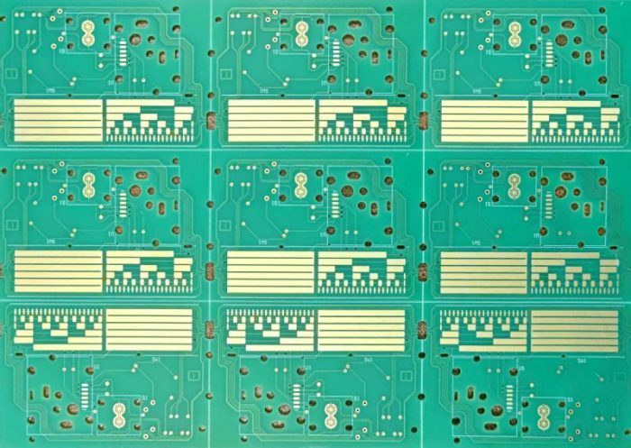
V-Cut Blank Printed Circuit Board
PCBs, especially rigid boards, cannot be broken apart manually without risking damage to components or substrate. V-Cut allows manufacturers to pre-weaken the board in a straight-line path, ensuring smooth, consistent separation.
This process reduces labor, minimizes component stress, and supports automated depaneling. For SMT-heavy or multi-board panels, V-Cut is often the preferred choice.
Jerico Multilayer PCB leverages advanced machinery to improve the quality and speed of V-Cut-based panelization:
Stamp Hole, also called Mouse Bite, is another method to connect PCBs in a panel. It uses a row of small drill holes (typically 0.5–0.8mm in diameter) to partially link the PCBs. Once assembly is complete, the panel is manually snapped or separated with pliers.
This technique is particularly u
Small Quantity PCB Manufacturer
seful when straight V-cuts are not possible due to the board shape.
| Feature | V-Cut | Stamp Hole (Mouse Bite) |
|---|---|---|
| Panel Separation Path | Straight only | Any shape, including curves |
| Automation Friendly | High | Low |
| Burr Formation | Minimal | Moderate to High |
| Mechanical Stress | Low | Higher due to manual breaking |
| Suitable for Thin PCB | Not recommended <1.0mm | Suitable for 0.6–2.0mm boards |
| Edge Quality | High | Rough, may need sanding |
| Cost | Low | Medium |
If your design is rectangular, over 1.0mm thick, and targeted for SMT production, V-Cut is the better option. If your PCB design is irregular, contains curves, or is too thin for V-Groove integrity, Stamp Hole may be more appropriate.
Jerico Multilayer PCB can produce both V-Cut and Stamp Hole boards based on customer needs, and can offer a hybrid panel structure to combine both technologies on a single panel where required.
Q1: Can I use V-Cut on a 0.8mm thick PCB?
A1: It is not recommended. At this thickness, the residual structure becomes weak and may cause breakage or warping during reflow.
Q2: Do Stamp Holes affect solder joint integrity?
A2: If the hole area is too close to SMT pads, the manual breaking force can stress or crack joints. Proper spacing and bridge design are essential.
Q3: Can I use both V-Cut and Stamp Hole in one panel?
A3: Yes. For complex designs, a hybrid approach is often used to optimize panel strength and separation convenience.
Q4: What is the lead time for V-Cut panels at Jerico?
A4: Single and double-layer boards can be delivered in 24 hours, while multilayer (4–6L) boards typically take 72 hours.
Q5: Does Jerico support full DFM and panel design review?
A5: Absolutely. Our engineers review Gerber files and provide free DFM optimization, including best-fit panelization strategy.
Still unsure which depaneling method is right for your PCB project? Contact Jerico Multilayer PCB supplier to get free consultation and a detailed recommendation tailored to your board layout and production volume.


Connect to a Jerico Multilayer PCB engineer to support your project!
Request A Quote


 Quote
Quote