


+86 13603063656
Understanding What Is a PCB Board is can completely transform how you approach electronic product development, prototyping, or sourcing. In today’s connected world, these silent green boards are at the heart of every modern device—from smartphones and laptops to cars and medical devices. But here’s the kicker… despite their importance, most professionals only scratch the surface when it comes to understanding how PCBs actually work. This article dives deep into the core of PCB technology, outlining its history, structure, types, and industrial applications. Whether you’re a buyer, engineer, or decision-maker in the electronics industry, this complete guide will give you everything you need to know.
What Is a PCB Board
Let’s start with the basics. PCB stands for Printed Circuit Board. It’s a flat board made of insulating material, usually fiberglass, with copper traces that create electrical connections. These boards act as the structural backbone for most electronic devices, supporting and wiring all the necessary components in place.
But this is where it gets interesting… PCBs aren’t just about connections. They’re engineered to manage heat, minimize interference, and optimize space, especially as electronics become smaller and more complex. From a business perspective, understanding what a PCB board is means making smarter sourcing and design decisions.
Whether you’re working with single-sided boards for simple gadgets or multilayer boards for advanced computing, the role of PCBs is indispensable. For manufacturers and OEMs, PCBs directly impact product size, weight, performance, and even safety compliance. That’s why choosing the right type of PCB—and understanding its anatomy—is critical in competitive markets.
| Key Term | Definition |
|---|---|
| PCB | Printed Circuit Board |
| Substrate | Base material that provides structure |
| Copper Trace | Conductive pathways for electricity |
| Solder Mask | Protective layer over copper |
| Silkscreen | Printed labels for components |
Believe it or not, the journey of PCB technology dates back to the early 1900s. German inventor Albert Hanson first proposed layered insulating boards with conductive paths. However, PCBs didn’t take off until after WWII, when Paul Eisler, an Austrian engineer, created the first true printed circuit board for a radio.
Fast forward to the 1950s, and PCB technology began entering commercial electronics. But here’s the real game-changer… the shift from point-to-point wiring to printed circuits revolutionized mass production. Not only did this reduce errors and improve consistency, but it also slashed assembly times.
By the 1980s, multilayer PCBs were becoming standard in computing and telecom. Today, thanks to surface mount technology (SMT), PCBs can house thousands of components on both sides of the board. As devices continue to shrink, HDI (High-Density Interconnect) PCBs are taking over, packing more power into smaller footprints.
| Timeline | Innovation |
|---|---|
| 1903 | Early concept of PCBs by Albert Hanson |
| 1943 | Paul Eisler invents modern PCB |
| 1950s | PCBs enter consumer electronics |
| 1980s | Multilayer PCBs gain popularity |
| 2000s | Surface Mount Technology and HDI emerge |
A PCB board is a mechanical structure that holds and connects electronic components using copper tracks instead of wires. But what’s the real story? A PCB doesn’t just connect parts—it controls how electricity flows and ensures the device works safely and efficiently.
Each PCB consists of multiple layers: the core substrate, a copper layer for signal pathways, solder mask to prevent shorts, and a silkscreen for labeling. Components like resistors, capacitors, and ICs are mounted on top and soldered to the copper pads.
Think of it this way: without a PCB, you’d have a tangled mess of wires, increasing the risk of failure, overheating, or poor performance. That’s why engineers rely on PCBs to design sleek, functional, and compact electronics.
| PCB Layer | Function |
|---|---|
| Substrate | Provides mechanical support |
| Copper Layer | Conducts electrical signals |
| Solder Mask | Prevents accidental solder bridges |
| Silkscreen | Prints labels and component info |
| Components | Mounted to create functionality |
Now we’re getting into the guts of a PCB. The structure of a PCB includes several layers and components that serve distinct roles.
First, we have the substrate—typically FR4, which is known for its durability and insulating properties. Above that lies the copper layer, where all the circuit pathways are etched. Then comes the solder mask, that green (or sometimes red, black, or blue) coating that protects copper traces from corrosion and soldering mistakes.
But here’s where it gets detailed… There are also vias (tiny holes that connect layers), pads (metallic points for soldering components), and traces (the “wires” of the board). Together, these allow you to build a complex circuit without ever using traditional wires.
| Component | Role in PCB |
|---|---|
| Via | Connects different layers electrically |
| Pad | Soldering point for components |
| Trace | Conducts electricity |
| Solder Joint | Mechanical/electrical bond |
| Mounting Hole | Secures PCB to enclosure |
Let’s peel back the layers—literally. A PCB works by creating a controlled environment for electrical currents to travel from one component to another. These currents are guided by copper traces that link various elements on the board.
Ready for the good part? Each trace is carefully calculated to carry a specific current, avoid interference, and deliver power or data precisely. When you power on a device, electrons travel through these paths, activating components like microprocessors, LEDs, and sensors.
Not just that—PCBs also help distribute heat, filter noise, and protect signals. In RF or high-speed applications, signal timing and impedance control are key, and a well-designed PCB can make or break the final product.
| PCB Function | Description |
|---|---|
| Signal Routing | Directs electrical signals between components |
| Power Distribution | Delivers stable power supply |
| Heat Management | Dissipates heat to prevent damage |
| Grounding | Ensures safe operation |
| EMI Shielding | Minimizes signal interference |
Here’s where the versatility of PCBs truly shines. Depending on the complexity of the application, PCBs come in various types.
Single-sided PCBs are the simplest. They feature copper on one side and are used in calculators or remote controls. Double-sided PCBs step things up by adding copper on both sides, allowing for more complex routing.
But here’s the kicker… Multilayer PCBs—ranging from 4 to 40+ layers—stack multiple substrates and copper layers, enabling high-speed, compact, and high-function designs. Then you’ve got flexible PCBs that bend, rigid PCBs that are solid, and rigid-flex that combine both for hybrid applications like aerospace or medical.
| PCB Type | Use Case |
|---|---|
| Single-sided | Simple, low-cost gadgets |
| Double-sided | Consumer electronics, power supplies |
| Multilayer | Computers, servers, telecom |
| Flexible | Wearables, mobile devices |
| Rigid-Flex | Aerospace, military, medical |
Material choice isn’t just a technical detail—it defines everything from board stability to thermal performance. So what are PCBs made of?
At the core is the substrate, usually FR4 (a glass-reinforced epoxy laminate), known for its electrical insulation and flame resistance. But there’s more… High-performance PCBs may use materials like polyimide for flexibility or aluminum for heat dissipation in LED applications.
Next comes the copper foil, which forms the conductive layers. This copper is typically 1 oz/ft² but can go thicker for high-current applications. The solder mask—often green—protects the copper, while the silkscreen helps with labeling.
| Material | Application |
|---|---|
| FR4 | Standard rigid PCBs |
| Polyimide | Flexible PCBs |
| Aluminum | High-heat applications (LEDs) |
| CEM-1 | Low-cost alternatives |
| Rogers | High-frequency boards |
Let’s talk design—because it all starts here. PCB design is the blueprint that dictates the board’s functionality and manufacturability. Using software like Altium Designer, Eagle, or KiCad, engineers create both the schematic and PCB layout.
What’s the real story? Every trace, via, and component placement is planned to avoid interference, manage heat, and ensure reliability. Engineers must follow design for manufacturability (DFM) guidelines to avoid costly mistakes down the line.
Even simple designs require attention to trace width, via spacing, and return paths. For multilayer designs, stack-up planning becomes essential to control impedance and reduce cross-talk.
| Design Element | Importance |
|---|---|
| Trace Width | Determines current-carrying capacity |
| Via Placement | Affects signal integrity |
| Stack-Up | Controls impedance and EMI |
| DRC Rules | Prevent layout errors |
| Component Orientation | Simplifies assembly |
Now let’s get our hands dirty. The PCB manufacturing process is a meticulous journey, turning your digital design into a physical board. It all starts with the design files, usually in Gerber format, which tell the manufacturer exactly what to build.
But here’s where it gets interesting… The process involves multiple steps: copper is laminated onto the substrate, and unwanted copper is etched away, leaving behind the circuit pattern. Next, holes are drilled and plated to form vias. The board is then covered with a solder mask and silkscreen before going through electrical testing.
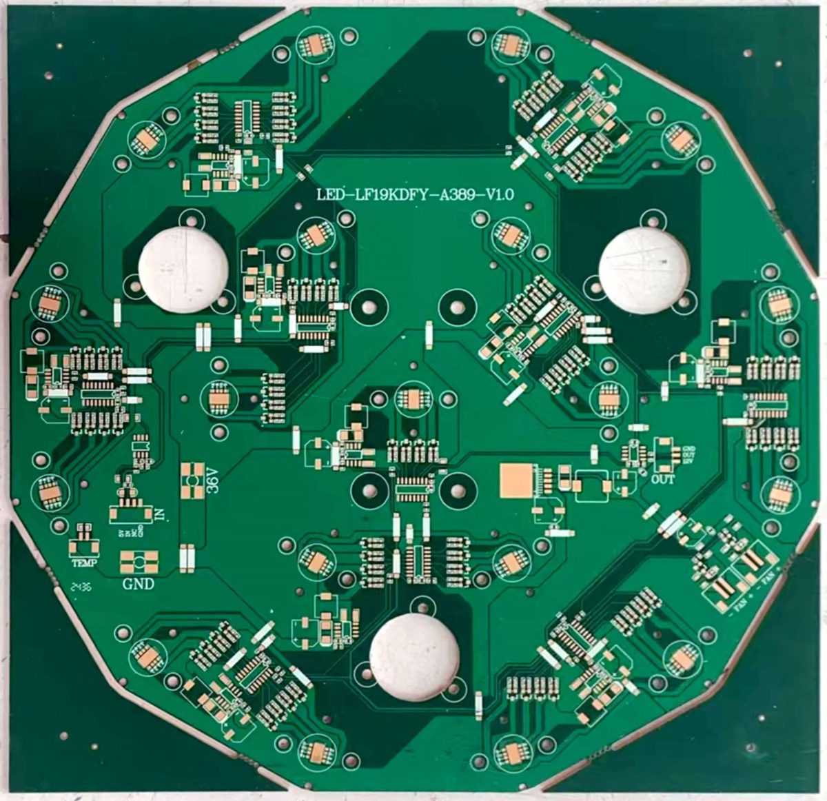
Precision is everything. A small error in drilling or copper etching can render the whole batch unusable. That’s why top-tier PCB suppliers like Jerico Multilayer PCB use automated inspection and quality control at every stage.
| Manufacturing Step | Purpose |
|---|---|
| Lamination | Bonds copper to substrate |
| Drilling | Creates vias and mounting holes |
| Etching | Removes excess copper |
| Plating | Adds conductivity to holes |
| Solder Mask | Protects copper traces |
So you’ve got a bare board—now what? This is where PCB assembly comes in. It’s the process of placing and soldering components onto the board, and it’s often more complex than the fabrication itself.
There are two main methods: Surface Mount Technology (SMT) and Through-Hole Technology (THT). SMT is more common for modern electronics because it’s faster and allows for miniaturization. In SMT, a stencil applies solder paste, pick-and-place machines position components, and a reflow oven solders everything in place.
But here’s the kicker… Assembly doesn’t end at soldering. The final board goes through AOI (Automated Optical Inspection), functional testing, and sometimes X-ray to catch hidden defects. Every step ensures the PCB functions perfectly before shipping.
| Assembly Method | Description |
|---|---|
| SMT | Small components mounted on surface |
| THT | Leads inserted through holes |
| Reflow Soldering | Heats solder paste to form joints |
| AOI | Detects placement and solder issues |
| ICT | Electrical testing for circuits |
PCBs are everywhere. In fact, it’s hard to find an electronic device that doesn’t rely on one. From your morning coffee machine to your car’s ABS system, PCBs are the quiet heroes.
Let’s break it down. In consumer electronics, PCBs power smartphones, TVs, and laptops. In automotive, they manage everything from engine control to parking sensors. Medical devices rely on PCBs for imaging, diagnostics, and wearables.
And this is where it gets fascinating… PCBs are also embedded in military systems, satellites, factory robots, and power grids. Their versatility is what makes them one of the most critical components in our digital world.
| Industry | Example Applications |
|---|---|
| Consumer | Phones, tablets, appliances |
| Automotive | ECU, infotainment, ADAS |
| Medical | Pacemakers, scanners, monitors |
| Industrial | PLCs, robotics, sensors |
| Aerospace | Avionics, communication |
You don’t want surprises at the customer site—this is why PCB testing is vital. Every PCB must go through rigorous testing before it leaves the factory floor. Quality assurance prevents failure in the field, ensuring reliability and customer satisfaction.
Ready for the good part? Testing starts with visual inspection and progresses to AOI, in-circuit testing (ICT), and functional testing. For critical applications, burn-in tests simulate real-world conditions to ensure performance over time.
At Jerico, we believe in building quality from the inside out. That means checking each trace, each via, and each solder joint before calling it complete.
| Test Type | Purpose |
|---|---|
| AOI | Visual inspection of solder joints |
| ICT | Checks circuit continuity and resistance |
| Functional Test | Simulates real use cases |
| X-ray | Inspects hidden solder joints |
| Burn-In | Stresses board under load |
Choosing the right PCB is a business-critical decision. But how do you know what’s best? It depends on the application, environment, complexity, and budget.
Here’s the deal… For simple devices, a single-layer PCB may do. For high-speed computing, multilayer boards are essential. If the board will flex or twist, go with flex or rigid-flex. And don’t forget: if heat is an issue, look for aluminum or copper-core boards.
It’s also vital to consider your supplier’s capabilities. Can they handle fine-pitch BGA? Do they offer impedance control or HDI layers? A strong partnership with your PCB vendor can save you from costly redesigns later.
| Selection Criteria | Description |
|---|---|
| Layer Count | Impacts routing and density |
| Material Type | Affects thermal and electrical performance |
| Finish | ENIG, OSP, HASL depending on needs |
| Board Thickness | Influences strength and impedance |
| Application Environment | Temperature, moisture, vibration |
The PCB industry is on the move. New technologies are reshaping how we design and manufacture boards. So what’s next?
First, miniaturization is driving demand for HDI (High-Density Interconnect) PCBs. These pack more circuits into smaller areas using microvias and fine traces. Then there’s the shift to flex and stretchable electronics for wearables, smart textiles, and medical sensors.
But wait, there’s more… Sustainability is also gaining ground. Lead-free processes, recyclable substrates, and energy-efficient manufacturing are becoming standard. And in high-performance sectors, 5G-ready materials and embedded components are pushing the boundaries even further.
| Trend | Impact |
|---|---|
| HDI Boards | Supports compact, high-speed designs |
| Flexible PCBs | Enables new device form factors |
| Green Manufacturing | Reduces environmental impact |
| Embedded Components | Increases functionality per area |
| 5G Materials | Supports higher frequencies |
To wrap it up, understanding what a PCB board is gives you a massive advantage—whether you’re designing, sourcing, or troubleshooting electronic products. From its layered construction and manufacturing process to testing and application, every aspect of a PCB plays a role in product performance and reliability.
So here’s the takeaway… Always align your PCB choice with the application needs. Don’t cut corners on testing or material quality. And most importantly, work with a supplier who speaks your language—both technically and strategically.
When done right, your PCB becomes more than a circuit—it becomes a competitive edge.
Q1: What is a PCB board?
A PCB (Printed Circuit Board) is a flat board used to mechanically support and electrically connect electronic components using copper traces and insulating layers.
Q2: How does a PCB work?
A PCB works by guiding electrical signals between components using conductive copper paths, enabling the device to perform its functions safely and reliably.
Q3: What are the different types of PCBs?
Types of PCBs include single-sided, double-sided, multilayer, rigid, flexible, and rigid-flex boards, each designed for specific applications and environments.
Q4: Can I design a PCB myself?
Yes, with tools like KiCad, Altium, or Eagle, engineers and hobbyists can design their own PCBs, but proper knowledge of layout rules and electrical principles is essential.
Q5: How much does it cost to make a PCB board?
The cost varies by size, layer count, complexity, and quantity, ranging from a few dollars for basic prototypes to hundreds for advanced, multilayer industrial boards.


Connect to a Jerico Multilayer PCB engineer to support your project!
Request A Quote


 Quote
Quote