


+86 13603063656
Designing a high-performance printed circuit board (PCB) is no longer just about connecting components. With the rising demands of high-speed electronics, IoT devices, and high-frequency communication systems, the need for careful consideration of signal integrity and overall PCB performance has never been greater. Optimizing a PCB layout requires a blend of technical knowledge, practical experience, and understanding of how electronic signals behave on complex board structures.
This guide aims to provide a comprehensive roadmap on how to layout a circuit board, offering detailed principles, practical techniques, and insights from real-world applications. Whether you are a professional PCB designer, an engineer working on prototype development, or a student learning PCB design fundamentals, this guide covers the critical factors that influence both signal integrity and reliability.
We will explore:
The fundamental principles of PCB layout and signal routing
Power distribution, thermal management, and material selection
Design rules, best practices, and tools that help optimize your layout
Practical case studies, common mistakes, and advanced techniques
Recommendations for reliable PCB manufacturing, including why JM PCB is a trusted partner in high-performance board production
By the end of this guide, you will have a detailed understanding of how to layout a circuit board in a way that balances performance, reliability, and manufacturability, ensuring your designs are both efficient and robust.
How to Layout a Circuit Board
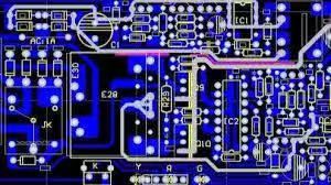
Before diving into advanced techniques, it is essential to understand the core concepts of PCB layout. At its essence, PCB layout is the process of transforming a schematic diagram into a physical board design where electronic components are interconnected by conductive traces.
The key objectives of a PCB layout include:
Signal Integrity: Ensuring that high-speed signals travel with minimal distortion or reflection.
Electrical Performance: Maintaining proper voltage levels, reducing noise, and managing power distribution effectively.
Mechanical Reliability: Ensuring the board withstands thermal and mechanical stress during operation.
Manufacturability: Designing a board that can be reliably produced within industry standards and cost constraints.
Understanding how to translate electrical schematics into a physical layout requires knowledge of the board materials, component types, and the physical behavior of signals on copper traces. Trace width, spacing, and layer selection all influence the final performance, particularly in high-speed designs where parasitic capacitance and inductance can affect signal quality.
Material selection plays a critical role in PCB performance. Standard FR-4 laminates are widely used for general-purpose boards due to their cost-effectiveness and mechanical stability. However, for high-frequency or high-speed applications, materials with controlled dielectric constants and low loss tangents, such as Rogers or Taconic laminates, can significantly improve signal integrity.
Component placement also affects both performance and manufacturability. Designers must consider:
Proximity of high-speed components: Minimize the length of critical signal paths.
Power and ground connections: Ensure low impedance paths for stable operation.
Thermal management: Place heat-generating components in locations that facilitate heat dissipation.
At this stage, it is also worth noting that working with a reliable manufacturer, such as JM PCB, can simplify material choices and ensure that your designs are executed with precision. They offer guidance on optimal stackups, trace widths, and advanced materials for signal integrity-critical boards.
The transition from schematic to layout involves mapping electrical connectivity into physical connections while considering real-world constraints. Key steps include:
Netlist Import: Most PCB CAD software allows designers to import the schematic netlist, which defines the electrical connections.
Component Footprint Assignment: Ensure footprints match actual components, including pin pitch and pad sizes.
Initial Placement: Arrange components to minimize critical trace lengths and separate noisy signals from sensitive analog paths.
Layer Planning: Decide on the number of signal layers, power planes, and ground planes based on board complexity.
Routing Strategy: Begin routing critical high-speed traces first, followed by secondary and low-speed signals.
Following these steps helps ensure that the final PCB layout maintains electrical performance while remaining manufacturable. The goal is not just connectivity, but optimization—reducing parasitic effects, minimizing EMI, and supporting the intended signal speeds.
Signal integrity begins with careful trace routing. The physical paths of your PCB traces determine how signals propagate and interact with other signals. Some key strategies include:
Shortest Path Routing: High-speed signals should travel along the shortest possible path to minimize delay and potential interference.
Consistent Trace Widths: Maintaining uniform trace width helps control impedance and reduces reflections.
Right-Angle Avoidance: Sharp 90-degree bends can create impedance discontinuities and signal reflections. Use 45-degree angles or curved traces instead.
Separation of Analog and Digital Signals: Isolate sensitive analog traces from noisy digital lines to prevent unwanted coupling.
Proper routing is not just about electrical performance but also manufacturability. Dense routing can increase fabrication complexity and cost, while excessive separation can make boards unnecessarily large. Optimizing the routing strategy is a balancing act between performance, cost, and layout constraints.
Crosstalk and electromagnetic interference (EMI) are common issues in high-speed PCB designs. Crosstalk occurs when signals on adjacent traces induce unwanted voltages, while EMI arises from radiated signals affecting other circuits. Effective management includes:
Trace Spacing: Maintain adequate spacing between high-speed traces to minimize capacitive and inductive coupling.
Ground Plane Utilization: Continuous ground planes under signal layers provide return paths and reduce EMI susceptibility.
Shielding Sensitive Components: Place sensitive analog components away from high-frequency switching circuits or consider adding ground shields.
Routing Critical Signals First: Route clock lines, high-speed data, and sensitive signals before less critical traces.
A practical insight is that proper EMI and crosstalk management often requires multiple iterations and simulation. Many designers use signal integrity tools to identify potential problems before fabrication, saving both time and cost.
Differential pairs are widely used for high-speed data transmission, such as USB, HDMI, and PCIe. Correct differential pair routing is critical for minimizing signal degradation:
Matched Lengths: Both traces in a differential pair must have equal lengths to prevent skew, which can distort the signal.
Controlled Impedance: The trace width, spacing, and layer stackup determine the differential impedance. Maintaining proper impedance ensures signal integrity over long traces.
Minimize Via Usage: Each via introduces impedance discontinuities, so use them sparingly in critical differential pairs.
Reference Plane Consistency: Differential pairs should be routed over a continuous reference plane to provide a stable return path.
Impedance control is equally important for single-ended signals. Designers often rely on manufacturer-provided stackup and trace calculators. At this stage, collaborating with experienced manufacturers, such as JM PCB, can ensure that impedance targets are met and high-frequency performance is reliable. Their expertise in material selection, layer stackup, and trace width recommendations makes them a valuable partner in high-performance PCB design.
Power integrity is as critical as signal integrity. Improper power distribution can lead to voltage drops, noise, and even circuit malfunction. Key strategies include:
Dedicated Power and Ground Planes: Use solid planes rather than traces for critical power nets to reduce impedance and provide low-resistance paths.
Layer Stackup Planning: Position power and ground planes adjacent to signal layers to create controlled impedance and minimize loop areas.
Power Partitioning: For boards with multiple voltage domains, separate power planes for each domain to reduce cross-domain interference.
Minimize Via Impedance: When connecting planes through vias, ensure sufficient via count and diameter to maintain low inductance.
Proper power plane design ensures stable voltage supply across the PCB and minimizes high-frequency noise, which is essential for high-speed circuits.
Decoupling capacitors play a vital role in maintaining local power integrity and reducing high-frequency noise. Proper placement and selection are crucial:
Close to IC Pins: Place decoupling capacitors as close as possible to the IC power pins to minimize loop inductance.
Multiple Values: Use capacitors of different values (e.g., 0.01 μF, 0.1 μF, 1 μF) to filter a wide frequency range of noise.
Direct Return Paths: Ensure a low-impedance path to ground planes for each capacitor.
Avoid Clustering: Spread capacitors across the board to ensure uniform power distribution.
Effective decoupling reduces voltage fluctuations and enhances overall signal integrity. Careful consideration of capacitor placement and plane connectivity is essential in both high-speed digital and sensitive analog designs.
High-performance components generate heat that can affect both reliability and signal integrity. Thermal management is a critical aspect of PCB layout:
Thermal Vias: Use arrays of vias to transfer heat from hot components to inner planes or heatsinks.
Copper Pours: Increase copper thickness or area around high-power components to enhance heat dissipation.
Component Placement: Avoid clustering heat-generating components; provide airflow paths for forced or natural convection.
Thermal Relief Pads: Ensure proper solderability while maintaining good thermal conduction for surface-mount and through-hole components.
In addition to protecting components, effective thermal management maintains electrical stability. Temperature gradients can cause impedance variations and introduce noise, especially in sensitive high-speed circuits. Designers must balance thermal, electrical, and mechanical requirements to achieve optimal performance.
Layer stackup is a fundamental factor in high-performance PCB design. It affects signal integrity, impedance control, EMI suppression, and manufacturability. When planning a multi-layer PCB:
Signal and Reference Plane Pairing: Each high-speed signal layer should be adjacent to a reference plane (ground or power) to maintain controlled impedance and minimize return path discontinuities.
Symmetric Stackup: Ensure the stackup is symmetrical to prevent warping and mechanical stress during fabrication.
Minimize Plane Splits: Avoid splitting ground or power planes unnecessarily, as discontinuities can increase impedance and EMI.
Consider Layer Count vs. Cost: While more layers provide better separation of signals, power, and ground, they increase fabrication cost. Optimize based on performance requirements.
Proper stackup planning balances signal integrity, thermal management, mechanical stability, and cost efficiency. Many designers rely on manufacturer guidance to select optimal stackups for high-speed or high-frequency boards.
Signal layer placement is closely linked to stackup decisions. Correct placement reduces crosstalk, minimizes EMI, and maintains signal integrity:
High-Speed Signals on Internal Layers: Place critical signals between reference planes to shield them from external noise.
Separate Analog and Digital Layers: Isolate analog signals from high-speed digital signals to prevent interference.
Routing Priority: Route clock lines and other high-speed signals first, followed by power-sensitive and low-speed traces.
Avoid Layer Transitions: Minimize layer changes for critical signals to reduce impedance discontinuities caused by vias.
Signal layer planning requires careful coordination with component placement, trace routing, and power distribution to achieve the desired performance.
High-speed and high-frequency designs present unique challenges. Techniques to maintain signal integrity include:
Controlled Impedance Traces: Design trace width and spacing according to the desired impedance using PCB calculator tools.
Differential Pairs and Matched Lengths: Ensure equal path lengths for high-speed differential signals to minimize skew.
Via Minimization: Each via introduces capacitance and inductance, which can degrade high-frequency signals.
Return Path Continuity: Always provide continuous return paths under signal traces to reduce EMI and signal degradation.
Termination Techniques: Use series or parallel terminations for signal reflections control in high-speed buses.
For complex high-speed boards, simulation tools are invaluable for predicting signal behavior before fabrication.
Maintaining proper spacing and clearance between traces, pads, and components is fundamental to ensure both electrical performance and manufacturability. Key considerations include:
Minimum Trace-to-Trace Spacing: Prevent short circuits and reduce capacitive coupling by following manufacturer-specified minimum spacing rules.
Pad-to-Trace Clearance: Ensure adequate clearance around pads to avoid solder bridging during assembly.
High-Voltage Considerations: For circuits with high-voltage lines, increase spacing to prevent arcing and maintain safety standards.
Thermal and Mechanical Factors: Proper spacing also helps with heat dissipation and reduces stress concentration in multilayer boards.
Following spacing guidelines protects both the board and components during operation and production, ensuring long-term reliability.
Vias are critical for interconnecting layers in multi-layer PCBs, but they introduce electrical and thermal considerations. Effective via management includes:
Via Size and Type: Choose appropriate through-hole, blind, or buried vias based on signal criticality and manufacturing capabilities.
Via Placement: Avoid placing vias in critical signal paths or beneath sensitive components to minimize impedance disruptions.
Thermal Vias: Use via arrays under heat-generating components to transfer heat to inner planes or heatsinks efficiently.
Minimize Via Count in High-Speed Paths: Each via introduces inductance and capacitance, which can degrade high-frequency signals.
Well-managed via placement ensures electrical integrity, thermal efficiency, and manufacturability.
Design for Manufacturability (DFM) ensures that your PCB layout can be reliably produced without errors or excessive cost. Key principles include:
Component Placement: Arrange components to simplify assembly and inspection. Avoid placing components too close to board edges or obstructing vias.
Panelization Considerations: Design boards with production panels in mind to reduce fabrication complexity and improve yield.
Solder Mask and Silkscreen: Apply clear solder mask openings and legible silkscreen labels to minimize assembly errors.
Avoid Overly Complex Routing: Excessively dense or intricate routing increases fabrication risk and may reduce yield.
DFM is a bridge between design and production, ensuring your layout translates seamlessly into a manufacturable board.
Effective PCB layout is a cornerstone of electronic design, directly impacting signal integrity, power distribution, thermal management, EMI/EMC performance, and overall reliability. Throughout this guide, we have explored the principles, strategies, and advanced considerations for how to layout a circuit board to achieve optimal performance. By integrating these principles, designers can produce PCBs that not only meet electrical specifications but also withstand the demands of modern electronics in terms of reliability, manufacturability, and thermal stability.
Ultimately, mastering how to layout a circuit board is a blend of science and practical experience. Understanding the interplay between electrical, thermal, mechanical, and manufacturing considerations allows engineers to optimize every aspect of their PCB, ensuring the final product performs as intended under real-world conditions.
Rolled copper foil is produced by mechanically rolling copper into thin sheets. This process results in a smoother surface finish and better mechanical strength, making it ideal for high-density interconnect (HDI) boards and fine-pitch components.
Electrolytic copper foil, on the other hand, is deposited via an electrolytic process. It is generally more flexible and cost-effective but may have slightly lower surface quality and mechanical strength. Choosing the correct foil type depends on your PCB’s electrical performance, mechanical stress tolerance, and manufacturing requirements.
Impedance control is critical for maintaining signal integrity in high-speed circuits. It involves managing the trace width, spacing, and proximity to reference planes (ground or power).
Differential Pairs: Match trace lengths to prevent skew and maintain differential impedance.
Simulation Tools: Use SI simulation software to calculate and verify impedance before fabrication.
Layer Stackup: Proper stackup design ensures consistent impedance across the board.
Decoupling capacitors stabilize local voltage levels and filter high-frequency noise, protecting sensitive ICs and maintaining power integrity.
Placement: Place capacitors as close as possible to IC power pins.
Multiple Values: Use a combination of capacitance values to cover a wide frequency range.
Ground Return: Ensure a low-inductance path to the ground plane.
Proper decoupling improves signal integrity and reduces voltage fluctuations across the board.
Minimizing EMI requires a combination of layout strategies and component placement:
Continuous Ground Planes: Provide proper return paths for high-speed signals.
Separation of Signal Types: Isolate digital, analog, and RF signals.
Differential Routing: Use differential pairs for high-speed signals to cancel radiated emissions.
Filtering: Incorporate ferrite beads, capacitors, and shielding where necessary.
Ensuring manufacturability involves adhering to DFM principles and collaborating with experienced manufacturers:
Design Rule Checks (DRC): Verify trace width, spacing, and via sizes against fabrication limits.
Panelization Considerations: Optimize board shape and panel layout for efficient assembly.
Component Placement and Accessibility: Allow adequate spacing for soldering and inspection.


Connect to a Jerico Multilayer PCB engineer to support your project!
Request A Quote


 Quote
Quote