


+86 13603063656
In the rapidly evolving world of electronics, the design and manufacturing of printed circuit boards (PCBs) are no longer simple exercises in connectivity. Every aspect of a PCB—its material, layer count, copper weight, and notably its thickness—plays a decisive role in performance, reliability, and cost. Choosing the appropriate PCB Board Thickness is a challenge that involves balancing electrical performance, mechanical strength, thermal management, and manufacturability (DFM), all while keeping the project within budget.
PCB designers often face the “thickness dilemma”: too thin a board may compromise structural integrity and heat dissipation, while too thick a board increases material cost and may complicate signal routing. Therefore, understanding the technical, economic, and functional implications of PCB board thickness is essential for engineers seeking optimal designs.
In this article, we explore the concept of PCB Board Thickness, provide guidance on choosing the right thickness for various applications, and offer practical insights into balancing cost, function, and manufacturability. Additionally, we will recommend JM PCB as a trusted provider for advanced PCB solutions.

PCB Board Thickness
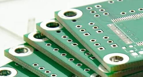
PCB Board Thickness refers to the overall vertical height of the printed circuit board, typically measured from the top to the bottom surface. It includes the base material (usually FR-4, polyimide, or other specialized substrates) and the copper layers on both sides. Thickness is usually expressed in millimeters or mils (1 mil = 0.001 inches).
Understanding thickness is crucial because it influences multiple factors:
Electrical properties: Impedance, capacitance, and signal integrity are partially determined by board thickness.
Mechanical strength: Thicker boards can withstand bending, vibration, and handling stresses better.
Thermal performance: Thicker boards can dissipate heat more effectively, which is critical in high-power applications.
Several factors determine the optimal PCB Board Thickness:
Application requirements: High-frequency circuits, RF modules, and power electronics may demand specific thickness ranges.
Layer count: Multilayer boards require precise control of individual layer thicknesses to maintain signal integrity.
Copper weight: Heavier copper layers (measured in oz/ft²) increase overall thickness and improve current-carrying capacity.
Mechanical constraints: Devices with tight space requirements may necessitate thinner boards, whereas industrial boards may require thicker ones for robustness.
Industry standards provide typical PCB thickness ranges:
Single-sided or double-sided boards: 0.4 mm to 1.6 mm (16 mils to 63 mils)
Multilayer boards: 0.8 mm to 3.2 mm (31 mils to 126 mils)
Flexible boards: 0.1 mm to 0.5 mm (4 mils to 20 mils), depending on the number of layers
These standards help designers select a starting point, but specific requirements may dictate deviations from standard thicknesses.
The choice of substrate material significantly affects PCB Board Thickness and overall performance:
FR-4: Standard for most applications; thickness varies with the number of layers and copper weight.
Polyimide: Used for flexible PCBs; enables thinner designs while maintaining mechanical and thermal performance.
Specialty materials: Rogers, ceramic, or metal-core substrates allow precise thickness optimization for high-frequency or high-thermal applications.
While thinner boards may save material costs, they can increase assembly difficulty and reduce durability. Conversely, thicker boards may provide reliability but increase costs and complicate high-density routing. Finding a balance is the essence of the thickness dilemma.
Signal integrity is one of the most critical aspects of modern PCB design, particularly in high-speed circuits. The PCB Board Thickness influences the impedance of traces, crosstalk between adjacent lines, and overall signal propagation.
Impedance control: The distance between signal layers and reference planes depends on board thickness. Variations in thickness can alter impedance, potentially causing signal reflections or timing errors.
Crosstalk reduction: Thicker boards can provide more spacing between traces on different layers, reducing unwanted coupling and noise.
High-frequency performance: At GHz frequencies, even small deviations in PCB thickness can degrade performance. Designers must carefully balance layer spacing with material properties.
Practical Tip: For controlled impedance designs, always specify the total PCB Board Thickness to the manufacturer and include stack-up diagrams in the design documentation.
Heat dissipation is another key consideration affected by PCB Board Thickness. Thicker boards generally offer better thermal paths, allowing heat to spread from components and prevent hotspots.
Power electronics: High-current traces benefit from increased copper thickness and overall board thickness, improving current-carrying capacity and reducing thermal stress.
Multilayer boards: Thermal vias combined with appropriate board thickness help dissipate heat efficiently.
Flexible PCBs: Thin flexible boards have limited thermal management capability, requiring careful design of copper layers and heat-spreading solutions.
Insight: The choice of thickness should consider both electrical and thermal requirements. Inadequate thickness may lead to overheating and reliability issues, especially in power-dense designs.
In high-speed digital or RF applications, the PCB Board Thickness plays a decisive role:
Signal propagation delay: Thicker boards increase trace separation, affecting propagation speed.
Impedance mismatch: Variations in thickness can introduce reflections, jitter, and signal degradation.
EMI and shielding: Proper board thickness helps maintain adequate spacing between layers, reducing electromagnetic interference.
Signal integrity, thermal management, and high-speed circuit performance are all highly dependent on PCB Board Thickness.
Choosing the correct thickness requires balancing electrical requirements, mechanical strength, and manufacturability.
Material and manufacturing costs are directly influenced by PCB Board Thickness:
Material cost: Thicker boards require more substrate and copper, increasing raw material expenses. For multilayer boards, additional layers compound this cost.
Manufacturing complexity: Thicker boards may require specialized drilling, lamination, and etching processes, which can raise production costs.
Assembly and testing: Thicker boards can handle heavier components more reliably, potentially reducing failures, but may also increase assembly time.
Designers must weigh the incremental cost of thicker boards against the benefits of improved mechanical strength, thermal performance, and signal integrity. A thin board may save immediate costs but could lead to higher failure rates and warranty expenses.
Choosing PCB Board Thickness is always a balancing act between functional requirements and cost constraints:
Thin boards: Ideal for lightweight and compact devices, such as mobile phones, wearables, and certain consumer electronics. They reduce material cost but may limit mechanical robustness and thermal dissipation.
Thick boards: Preferred in industrial, automotive, or high-power applications where durability, heat dissipation, and electrical stability are critical. The higher upfront cost can be justified by longer product life and reliability.
Evaluate the end-use environment and operational demands. The right thickness is not necessarily the thinnest or the thickest—it is the one that meets functional requirements without unnecessary expense.
Design for Manufacturability (DFM) is crucial when selecting PCB Board Thickness. Poor DFM decisions can lead to:
Drill misalignment or breakout: Thicker boards require precise drilling to avoid vias that do not meet tolerance.
Warping during lamination: Uneven thickness distribution may cause warping, especially in multilayer boards.
Soldering and assembly issues: Variations in board thickness can affect automated pick-and-place and reflow soldering processes.
When balancing cost, function, and DFM, JM PCB stands out as a reliable partner:
Customizable thickness solutions: JM PCB provides a wide range of substrate thicknesses, copper weights, and multilayer configurations.
Advanced engineering support: They assist in stack-up design, impedance control, and thermal management optimization.
Cost-effective manufacturing: With modern fabrication processes and lean production techniques, JM PCB ensures competitive pricing without compromising quality.
Leveraging JM PCB’s expertise allows designers to focus on performance and innovation, while ensuring that board thickness, reliability, and manufacturability are fully optimized.
Selecting the right PCB Board Thickness begins with understanding established standards:
IPC standards: IPC-2221 and IPC-6012 provide guidelines for thickness ranges based on board type, application, and reliability requirements.
Thickness vs. layer count: Single- and double-sided boards typically range from 0.4 mm to 1.6 mm, while multilayer boards can go up to 3.2 mm.
Tolerance considerations: Most manufacturers allow ±10% variation in thickness; critical high-speed or impedance-controlled designs may require tighter tolerances.
Following industry standards reduces risk and ensures that the board can be manufactured consistently across different suppliers.
Layer count and component density directly influence PCB Board Thickness:
Multilayer boards: Each additional layer adds substrate, dielectric, and copper, increasing overall thickness. Stack-up planning is essential to maintain impedance control.
High-density boards: Thinner boards may be preferable to minimize package height, but careful planning is needed to avoid thermal and mechanical issues.
Component placement: Heavy or tall components may require thicker boards for stability, especially in automotive or industrial applications.
Use simulation tools and collaborate with the manufacturer to determine the minimum board thickness that meets mechanical and electrical requirements.
Mechanical considerations are critical when choosing PCB Board Thickness:
Flexural rigidity: Thicker boards resist bending and warping, which is essential for large boards or those exposed to mechanical stress.
Vibration resistance: Industrial and automotive boards benefit from increased thickness to handle shock and vibration.
Long-term reliability: Thicker boards can reduce the risk of via or trace cracking over time, improving product lifespan.
While thin boards may reduce material cost, they can compromise long-term durability in high-stress environments. Evaluating mechanical requirements ensures a balanced design. The final device achieved optimal performance, mechanical reliability, and manufacturability while keeping production costs reasonable.
Flexible and rigid-flex PCBs introduce unique challenges when selecting PCB Board Thickness:
Flexibility vs. durability: Flexible boards must remain thin enough to bend without cracking copper traces or substrate layers, often ranging from 0.1 mm to 0.5 mm.
Layer distribution: In rigid-flex designs, thickness must be carefully controlled between rigid sections and flexible areas to maintain electrical and mechanical performance.
Stress management: Vias and components on flexible areas require precise thickness and copper distribution to prevent fatigue over repeated bending cycles.
High-power PCBs, such as those used in power converters, LED drivers, and industrial machinery, require special attention to PCB Board Thickness:
Current-carrying capacity: Thicker copper layers and overall board thickness reduce resistance, minimizing voltage drops and heating.
Thermal management: Adequate thickness allows for better heat spreading, particularly when combined with thermal vias and heat sinks.
Safety and reliability: Thicker boards reduce the risk of delamination, warping, or trace burnout in high-current conditions.
In high-power applications, overemphasis on cost savings through thinner boards can lead to catastrophic failure. Selecting the correct thickness ensures safety and long-term reliability.
Environmental conditions and regulatory compliance influence PCB Board Thickness decisions:
Temperature extremes: Aerospace, automotive, and outdoor electronics require boards thick enough to withstand thermal cycling without warping.
Moisture and corrosion: Proper thickness, combined with protective coatings, improves resistance to humidity and chemical exposure.
Regulatory standards: UL, RoHS, and IPC guidelines often dictate minimum thicknesses and material properties for safety and reliability.
Considering environmental factors early in design prevents costly redesigns and ensures compliance with regulatory standards.
Selecting the appropriate PCB Board Thickness is more than a technical specification—it is a strategic decision that influences electrical performance, thermal management, mechanical durability, and overall product reliability. Designers face a complex trade-off: thinner boards reduce material costs and allow compact designs, while thicker boards provide improved structural integrity, heat dissipation, and signal stability.
In conclusion, the “thickness dilemma” is not about choosing the thinnest or thickest PCB possible; it is about finding the optimal PCB Board Thickness that balances cost, function, and manufacturability. By combining technical knowledge, practical guidelines, and collaboration with experienced manufacturers such as JM PCB, designers can ensure that their PCBs meet both performance and reliability goals while staying within budget.
Final Insight: Every PCB design has unique demands, and there is no one-size-fits-all solution. Thoughtful selection of PCB Board Thickness, guided by standards, simulations, and manufacturer expertise, transforms potential trade-offs into optimized solutions—delivering robust, high-performance, and cost-effective electronics.
Rolled copper foil and electrolytic copper foil are two common types of copper used in PCBs, and they differ in production method and performance:
Rolled copper foil: Produced by mechanically rolling copper into thin sheets. It offers better surface quality, smoother texture, and higher mechanical strength, making it ideal for fine-line and high-density circuits.
Electrolytic copper foil: Deposited via an electrolytic process. It is more flexible, cost-effective, and suitable for multilayer boards where extreme mechanical strength is not critical.
Selecting the right copper type affects the overall PCB Board Thickness and functional reliability, particularly in high-speed or flexible PCB designs.
Impedance is determined by the geometry of traces, dielectric material, and distance to the reference plane.
Variations in PCB Board Thickness can change trace-to-plane spacing, potentially causing reflections, signal loss, or timing errors.
Controlled thickness ensures that impedance remains within design tolerances, critical for high-speed digital and RF circuits.
Always specify board thickness and stack-up to the manufacturer for precise impedance control.
Thinner boards reduce the separation between signal and reference planes, which can improve coupling in some high-frequency applications.
However, excessively thin boards may compromise mechanical strength and thermal performance, leading to warping or failure.
Balance is essential: select a thickness that optimizes high-frequency signal propagation without compromising durability.
Common mistakes include:
Ignoring mechanical requirements: Thin boards may warp or crack under stress.
Neglecting thermal performance: Insufficient thickness can cause hotspots and component failure.
Skipping manufacturer consultation: Not considering DFM constraints can result in fabrication challenges or higher costs.
Over-relying on standard thickness: Every application has unique electrical, thermal, and mechanical requirements.
Flexible and rigid-flex boards require careful thickness planning to maintain bendability while ensuring reliability.
Strategies include:
Using thinner substrates in flex regions.
Minimizing copper weight in bend areas.
Reinforcing rigid sections to provide stability without impacting flexible zones.
Simulation and prototype testing are essential to ensure that chosen thickness meets both functional and mechanical requirements.


Connect to a Jerico Multilayer PCB engineer to support your project!
Request A Quote


 Quote
Quote