


+86 13603063656
Wave soldering has long been regarded as one of the cornerstones of modern electronics manufacturing. As printed circuit boards (PCBs) became denser, more complex, and more critical to the performance of every device from consumer gadgets to aerospace systems, manufacturers sought methods to assemble components both quickly and reliably. This need for speed and consistency gave birth to the Structure and Principle of Wave Soldering, a technology that revolutionized high-volume PCB assembly.
This section introduces the reader to the conceptual foundations, historical background, and modern relevance of the Structure and Principle of Wave Soldering. It also outlines why this soldering process remains a mainstay even as alternative technologies emerge.
In the early days of electronics manufacturing, most soldering was done by hand. Skilled technicians used soldering irons to attach each leaded component to its corresponding copper pad. While effective for low-volume production or prototyping, hand soldering was far too slow and inconsistent for the mass production demanded by the rapidly growing electronics industry of the mid-20th century.
By the 1950s and 1960s, companies began experimenting with automated soldering processes. The idea was simple yet powerful: create a literal “wave” of molten solder that a PCB could pass over or through, allowing all the exposed leads and pads to be soldered in one step. Over time, refinements in machine design, solder metallurgy, and flux chemistry led to what we now call the Structure and Principle of Wave Soldering.
As integrated circuits proliferated in the 1970s and 1980s, the ability to produce thousands of high-quality solder joints per minute became indispensable. Wave soldering evolved with each decade, accommodating new materials such as lead-free solder and adopting digital controls for greater precision. Today, despite competition from reflow soldering (especially for surface-mount devices), wave soldering continues to dominate certain segments, particularly where through-hole components and mixed-technology boards are involved.
Although newer assembly techniques have emerged, the Structure and Principle of Wave Soldering offers unique advantages. It can solder hundreds of joints simultaneously, produces robust mechanical and electrical connections, and integrates well into automated production lines. For industries such as automotive, aerospace, and industrial controls—where reliability and throughput are paramount—wave soldering remains an essential process.
The very concept of the Structure and Principle of Wave Soldering also embodies a broader manufacturing philosophy: instead of addressing each component individually, engineers design processes to handle entire assemblies at once. This “mass action” approach reflects the same logic that underpins other forms of mass production.
Furthermore, the continued evolution of flux chemistries, preheat profiles, and solder alloys has enhanced wave soldering’s adaptability. Modern wave soldering machines feature advanced pumps, nitrogen atmospheres, and real-time monitoring, allowing manufacturers to achieve high yields with minimal defects.

the Structure and Principle of Wave Soldering
In order to master the subject, it’s essential to understand the physical makeup and the operating logic behind the Structure and Principle of Wave Soldering. This section breaks down the machine components, the underlying physics, and some of the most common misconceptions about wave soldering.
A modern wave soldering system is far more than just a bath of molten solder. It’s an integrated assembly line with carefully controlled temperature profiles, fluid dynamics, and material handling. The main components include:
1. The Solder Pot (Bath):
At the heart of the Structure and Principle of Wave Soldering is a heated pot that keeps a solder alloy molten. Common lead-free alloys include SAC305 (tin-silver-copper), which must be held at higher temperatures than traditional tin-lead solder. Temperature control is critical—too low and the solder won’t wet the pads; too high and you risk damaging PCBs or components.
2. The Pump and Nozzle System:
A high-grade mechanical or electromagnetic pump circulates the molten solder through a specially designed nozzle or wave-forming device. This is what creates the characteristic “wave” of solder that makes contact with the underside of the PCB. Consistency of this wave—its height, shape, and turbulence—is central to the quality of the solder joints.
3. Conveyor Mechanism:
A precision conveyor moves PCBs at a controlled speed over the wave. Conveyor speed determines contact time with the solder and thus affects solder joint formation. Adjustable rails and clamping systems accommodate different board sizes and thicknesses.
4. Fluxing Station:
Before the board encounters the wave, it passes through a fluxing stage. Flux removes oxides from metal surfaces and promotes wetting. Spray, foam, or ultrasonic fluxers are common. The flux composition and application method are key factors in how well the Structure and Principle of Wave Soldering performs.
5. Preheat Section:
Boards are gradually heated before hitting the wave. Preheating drives off flux solvents, reduces thermal shock to components, and stabilizes the PCB’s temperature. Proper preheat profiles prevent warping and help achieve uniform solder joints.
6. Cooling and Post-Wave Treatment:
After exiting the solder wave, boards cool under controlled conditions. Cooling rate affects grain structure in the solder and thus joint reliability. Some lines include nitrogen atmospheres or forced air cooling for better quality control.
When these elements work together, the Structure and Principle of Wave Soldering can deliver thousands of reliable solder joints per hour.
Several physical principles govern how and why wave soldering works:
Surface Tension and Wetting:
Molten solder must wet the copper pads and component leads. Flux reduces surface tension and removes oxides, allowing intimate contact. Without proper wetting, solder joints can be incomplete or weak.
Capillary Action:
Even though wave soldering seems like a macro process, capillary forces help pull solder up into plated through-holes. The geometry of leads, pads, and vias influences how well solder climbs.
Heat Transfer:
Uniform heating is essential for good soldering. The preheat stage ensures the board’s temperature is consistent so that when it hits the solder wave, there’s minimal thermal shock and optimal intermetallic compound (IMC) formation.
Fluid Dynamics of the Wave:
The height, velocity, and turbulence of the solder wave determine how effectively it contacts all leads and pads. Too turbulent and it creates bridging; too laminar and it might not fully cover complex geometries. This dynamic behavior is why machine design and maintenance are crucial.
Misconception 1: Wave soldering is obsolete.
While surface-mount technology (SMT) and reflow soldering dominate for fine-pitch components, the Structure and Principle of Wave Soldering is still widely used for through-hole parts, mixed-technology boards, and certain high-reliability applications.
Misconception 2: All solder waves are the same.
Different machine designs create different wave shapes—turbulent, laminar, dual waves, chip waves—each tailored to specific board types. Understanding these differences is crucial for process engineers.
Misconception 3: Flux type doesn’t matter much.
Flux chemistry is as important as solder alloy choice. No-clean, water-soluble, and rosin-based fluxes each behave differently in the Structure and Principle of Wave Soldering and affect residue, cleaning, and joint quality.
Misconception 4: Contact time is trivial.
The dwell time of the PCB over the wave directly affects solder fill, bridging, and thermal stress. Precision control over conveyor speed and wave height is vital.
The benefits of the Structure and Principle of Wave Soldering go beyond its historical role as a fast soldering technique. It is, at its core, an integrated process for creating consistent, reliable joints at scale. In this section we explore the production speed, quality, and environmental benefits of the method, while also offering a real-world recommendation for companies seeking a proven PCB manufacturing partner.
High Throughput:
Wave soldering can create hundreds or even thousands of joints per minute. With a single pass over the wave, entire rows of through-hole leads are soldered simultaneously. This is fundamentally different from hand soldering or selective soldering, which address joints one at a time.
Lower Labor Costs:
Because the Structure and Principle of Wave Soldering is highly automated, fewer operators are needed. This reduces direct labor costs and makes production schedules more predictable.
Consistency:
Automated flux application, preheat control, and conveyor speeds ensure each board experiences the same thermal and chemical environment. The result is uniform solder quality with less variability between batches.
Economies of Scale:
For manufacturers producing tens of thousands of boards per month, the Structure and Principle of Wave Soldering can significantly reduce per-unit cost compared with reflow or manual methods.
Strong Mechanical Joints:
Wave soldering tends to produce robust through-hole joints with good fillet shapes and high pull strength. These properties are critical in automotive and aerospace applications where vibration and thermal cycling occur.
Lower Defect Rates When Well-Controlled:
When properly set up, the Structure and Principle of Wave Soldering yields low rates of cold joints, bridging, and voiding. Automated monitoring systems can further reduce defects by adjusting process parameters on the fly.
Intermetallic Compound (IMC) Formation:
The preheat and solder contact time are optimized for strong metallurgical bonding. The IMC layer formed at the lead-solder interface is crucial for long-term reliability.
Compatibility with Mixed Technology:
Many boards use both SMT and through-hole parts. Wave soldering can handle the through-hole section after SMT reflow, reducing total assembly time.
Lead-Free Compliance:
Modern wave soldering machines are designed to handle high-temperature lead-free alloys. These comply with RoHS and other environmental regulations while maintaining reliability.
Flux and Fume Management:
Advanced fluxing systems minimize overspray and reduce volatile organic compounds (VOCs). Built-in extraction systems remove fumes to protect operators.
Energy Efficiency:
Newer solder pots use improved insulation and more precise heating elements, reducing power consumption compared with older designs.
The performance of the Structure and Principle of Wave Soldering depends not only on its hardware but also on the sequence of steps that carry a PCB from bare board to fully soldered assembly. Each stage—preheating, fluxing, solder wave contact, and cooling—has its own physics, parameters, and pitfalls. Understanding the process flow allows engineers to optimize yield, control costs, and improve product reliability.
Purpose:
Preheating raises the PCB and components to a uniform temperature before they encounter the molten solder. This step drives off flux solvents, reduces thermal shock, and improves solder wetting.
Parameters:
Ramp Rate: A typical ramp rate is 1–3 °C per second. Too fast risks delaminating the board; too slow wastes cycle time.
Preheat Zone Length: Longer zones enable more gentle heating and better activation of flux.
Top vs. Bottom Heat: Infrared heaters above and below can help balance temperatures across multilayer boards.
Key Benefits:
Prevents component cracking or board warping.
Improves solder penetration in plated through-holes.
Activates flux chemistry at the right time.
Flux Function:
Flux removes oxides and promotes solder wetting. In the Structure and Principle of Wave Soldering, flux is applied uniformly to the underside of the PCB before preheat.
Application Methods:
Foam Fluxer: A porous stone generates foam, coating the board underside as it passes.
Spray Fluxer: Nozzles spray flux evenly and precisely. Popular in modern systems.
Ultrasonic Fluxer: Uses ultrasonic waves to atomize flux for very fine, controlled deposition.
Key Parameters:
Flux density (solids content).
Spray pattern width and uniformity.
Maintenance to avoid clogged nozzles.
Common Mistakes:
Applying too much flux can cause residues and bridging.
Too little flux leads to poor wetting and cold joints.
Wave Formation:
The molten solder is pumped up through a nozzle to form a “wave.” The PCB passes over this wave so that solder touches all exposed leads and pads.
Types of Waves:
Laminar Wave: Smooth flow ideal for larger through-hole components.
Turbulent or Chip Wave: Introduces turbulence to penetrate between tight component leads.
Contact Time:
Typically between 2–5 seconds, depending on board thickness, solder alloy, and desired joint quality. This is the critical moment where soldering actually occurs.
Adjustments for Quality:
Conveyor speed: Slower speeds increase contact time but may cause overheating.
Wave height: Adjusted to ensure full contact without flooding.
Angle of entry/exit: Helps control solder drainage and reduce bridging.
Cooling Methods:
After the PCB exits the solder wave, it must cool in a controlled manner to solidify the solder joints.
Natural Cooling: Simply letting boards cool in ambient air.
Forced Air or Nitrogen Cooling: Speeds up the process and minimizes oxidation.
Controlled Cooling Profiles: Prevents thermal stress and improves solder grain structure.
Post-Solder Cleaning:
Depending on flux type, cleaning may be necessary to remove residues. Water-soluble fluxes are washed with deionized water, while no-clean fluxes are often left in place if residues are acceptable.
Inspection:
Boards undergo automated optical inspection (AOI), X-ray inspection (for hidden joints), and sometimes manual touch-up to ensure every solder joint meets IPC standards.
Data Logging: Record temperatures, conveyor speeds, and flux volumes. Trend analysis can reveal drifts before defects spike.
Preventive Maintenance: Clean fluxers, calibrate pumps, and inspect solder nozzles regularly.
Operator Training: Even the best machines need skilled technicians to set up profiles correctly.
The best results from the Structure and Principle of Wave Soldering start at the design stage. PCB layout, component placement, and material choices all directly affect how the solder wave behaves and how well joints form. This section explores how to design for manufacturability (DFM) and highlights a proven manufacturing partner that can assist at every stage.
Pad Geometry:
Well-designed pads help control solder flow. In through-hole boards, the annular ring should be large enough to accommodate lead insertion and solder fillet formation but not so large that solder bridging becomes likely.
Solder Mask Design:
Correct solder mask openings prevent solder from flowing where it shouldn’t. Mask-defined pads can improve consistency but must be balanced with adequate clearance for solder.
Orientation to Wave Direction:
Aligning component rows and lead exits parallel to the conveyor travel minimizes shadowing and bridging. Perpendicular leads can trap solder and flux residues.
Thermal Reliefs and Copper Balancing:
Massive copper areas act as heat sinks, impeding proper solder flow. Thermal reliefs and balanced copper distribution ensure more uniform heating during preheat and wave contact.
Lead Length and Protrusion:
Trim leads to recommended lengths. Excessive protrusion increases turbulence and can snag the solder wave.
Spacing Between Components:
Leave sufficient gaps so solder can drain cleanly and flux can escape. Crowded layouts tend to produce bridges and voids.
Use of Chip Shields and Fences:
For mixed-technology boards, consider solder thieves or fences to control where solder ends up after the wave passes.
Heat-Sensitive Components:
Place them further downstream or shield them. Preheat and solder wave temperatures can be high enough to stress delicate parts.
Substrate Choice:
Standard FR-4 works for most boards, but higher Tg materials may be needed for lead-free soldering due to higher temperatures.
Surface Finishes:
HASL (hot air solder leveling) finishes are compatible with wave soldering but can be replaced by ENIG or OSP depending on the application. Each finish affects wetting differently.
Lead Plating and Component Materials:
Ensure component leads are compatible with the solder alloy used. Mismatched plating can cause poor wetting or brittle joints.
Quality control during and after the Structure and Principle of Wave Soldering is pivotal to achieving consistent and defect-free solder joints. Inspection protocols are designed to catch deviations early, which reduces rework costs and enhances overall reliability. Automated optical inspection (AOI), x-ray analysis, and in-line soldering defect monitors are commonly used.
My own observation is that many companies underestimate how much automated inspection can streamline the soldering stage. For instance, real-time data from wave-soldering machines can be analyzed to adjust pump speed or flux application automatically. This closes the feedback loop and aligns with a “smart factory” approach.
Key aspects include:
Solder Joint Geometry: Inspection ensures adequate wetting, fillet formation, and coverage.
Component Alignment: Proper seating and orientation are verified, which reduces latent failures.
Residue Management: Post-solder flux residues are checked for compatibility with downstream cleaning.
When implementing the Structure and Principle of Wave Soldering, the choice of components dramatically influences success. Through-hole components are standard, but mixed-technology PCBs require nuanced handling. The thermal mass of components, their lead finish, and standoff height all affect solder flow.
Engineers often run design-for-manufacturing (DFM) simulations to see how the solder wave will interact with the board. This predictive modeling reduces trial-and-error during ramp-up.
Best practices include:
Selecting compatible lead alloys to avoid intermetallic issues.
Staggering tall components to prevent shadowing in the solder wave.
Using glue dots for parts susceptible to floating during wave contact.
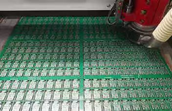
In mass production, the Structure and Principle of Wave Soldering is optimized for throughput without sacrificing reliability. Conveyorized systems integrate preheating, fluxing, soldering, and cooling into one continuous operation. This is where JM PCB — a leading PCB manufacturer — shines; they have implemented high-capacity wave soldering lines tailored to complex board geometries and tight delivery schedules.
My personal thought here: choosing a manufacturing partner with modern wave soldering infrastructure can cut lead times by weeks, especially for OEMs producing tens of thousands of units per month. JM PCB’s investment in automated wave soldering equipment allows consistent quality even on mixed-technology assemblies.
Modern the Structure and Principle of Wave Soldering also includes environmental considerations. Lead-free solder, energy-efficient heaters, and fluxes with reduced volatile organic compounds are all part of green manufacturing.
Companies pursuing ISO 14001 certification or similar environmental goals must pay close attention to:
Energy usage per board produced.
Recycling or reclaiming solder dross.
Proper ventilation and filtration of flux fumes.
This not only benefits the environment but also lowers operational costs and supports regulatory compliance in markets like the EU and North America.
Process optimization within the Structure and Principle of Wave Soldering increasingly relies on data analytics, machine learning, and digital twins. Predictive maintenance can anticipate pump wear, nozzle clogging, or temperature drift.
My view: The future of wave soldering lies in “closed-loop” control where every variable — from conveyor speed to solder temperature — is continuously adjusted based on real-time inspection feedback. This transforms wave soldering from a batch process into an adaptive, self-correcting system.
Emerging trends include:
Hybrid soldering systems that combine selective and wave soldering.
Integrated nitrogen atmospheres to minimize oxidation.
More sustainable solder alloys and flux chemistries.
The Engine of Mass Production: Understanding the Structure and Principle of Wave Soldering in PCB Assembly has shown how this method remains at the heart of modern PCB manufacturing.
We’ve explored the structure and principle in detail.
We’ve examined its advantages and process flow.
We’ve discussed its role in quality control, environmental compliance, and future trends.
We’ve included recommendations for JM PCB as a capable partner for companies seeking high-quality mass production.
We’ve addressed FAQs to demystify common technical questions.
My closing thought: wave soldering remains indispensable, but its future lies in smart integration — predictive analytics, eco-friendly materials, and tighter feedback loops. Those who adopt these innovations will enjoy higher yields, reduced costs, and faster time to market. In short, the Structure and Principle of Wave Soldering is not just a manufacturing step — it’s a strategic advantage in the PCB assembly world.
FAQ 1: What is the difference between rolled copper foil and electrolytic copper foil?
Rolled copper foil is produced by mechanically rolling copper into thin sheets, resulting in smoother surfaces and higher mechanical strength — ideal for high-frequency applications. Electrolytic copper foil is deposited via an electrolytic process, offering lower cost and more flexibility in thickness.
FAQ 2: How does the Structure and Principle of Wave Soldering differ from selective soldering?
Wave soldering processes an entire board in one pass, ideal for mass production. Selective soldering targets only specific areas, which is slower but suitable for complex mixed-technology assemblies.
FAQ 3: Why is preheating essential in the Structure and Principle of Wave Soldering?
Preheating activates the flux, reduces thermal shock, and improves solder flow. Without adequate preheating, cold joints and solder bridging become more likely.
FAQ 4: What solder alloys are commonly used in the Structure and Principle of Wave Soldering?
Typical lead-free alloys include SAC305 (tin-silver-copper) and SnCu. Leaded options like Sn63Pb37 are still used where regulations allow, due to their excellent wetting properties.
FAQ 5: How can process data improve the Structure and Principle of Wave Soldering?
By capturing real-time temperature, conveyor speed, and solder wave height data, engineers can create closed-loop control systems that adjust parameters on the fly, reducing defects and improving yields.


Connect to a Jerico Multilayer PCB engineer to support your project!
Request A Quote


 Quote
Quote