


+86 13603063656
As signal speeds climb into multi-gigahertz ranges and RF frequencies push higher with each generation of wireless technology, the printed circuit board has evolved from a passive interconnect platform into an active participant in electrical performance. Among the many design parameters that quietly but decisively shape high-speed and RF behavior, Antipad Clearance stands out as one of the least visible yet most influential factors.
In traditional PCB design, antipads were often treated as simple geometric necessities—clearances drilled or etched to isolate vias and pads from internal copper planes. However, in modern multilayer PCB manufacturing, especially for high-speed digital and RF applications, Antipad Clearance directly influences impedance control, signal integrity, crosstalk, EMI behavior, and even long-term reliability.

Antipad Clearance
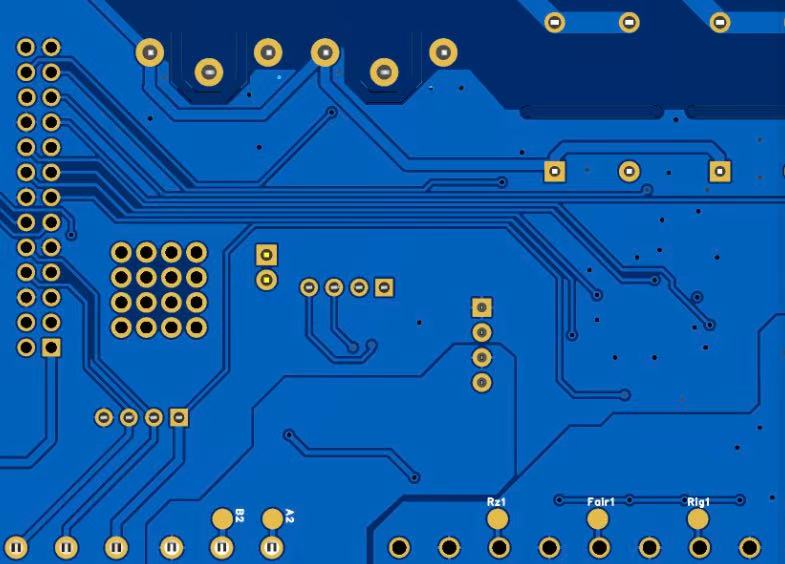
Antipad-Clearance refers to the intentional copper void created around a plated through-hole, via, or pad where it passes through a copper plane layer. Unlike pads, which provide electrical connectivity, antipads provide electrical isolation.
From a purely geometric standpoint, Antipad Clearance defines:
The diameter of copper removed around a via or hole
The spacing between the via barrel and plane copper
The local discontinuity within an otherwise continuous reference plane
Electrically, however, Antipad-Clearance behaves as more than empty space. It forms a capacitive and inductive discontinuity that alters how electromagnetic fields propagate around the via transition.
In multilayer PCBs, vias often traverse multiple reference planes. Each plane crossing introduces an antipad, and collectively these antipads form a via channel with cumulative electrical effects.
From my experience, designers frequently optimize trace impedance but overlook the fact that vias with poorly controlled Antipad Clearance can dominate overall signal degradation, especially in:
High-speed serial links (PCIe, USB4, Ethernet)
RF front-end modules
High-frequency clock distribution networks
Many CAD tools default Antipad-Clearance to conservative values. While safe, these defaults are rarely optimal. Treating Antipad Clearance as a static rule rather than a tunable parameter often leads to:
Excessive via capacitance
Impedance dips at layer transitions
Unpredictable return current paths
Understanding Antipad-Clearance as an impedance-shaping feature is the first step toward advanced PCB optimization.
A via behaves like a short transmission line. Its impedance is strongly influenced by:
Drill diameter
Plating thickness
Antipad Clearance size
Dielectric constant of surrounding material
Smaller Antipad-Clearance increases parasitic capacitance, lowering via impedance. Larger Antipad-Clearance reduces capacitance but may increase inductive effects and plane disruption.
In high-speed designs, I’ve observed that even a 2–3 mil change in Antipad Clearance can shift eye diagrams from marginal to compliant.
High-speed signals always travel with return currents. When a signal via transitions layers, the return current must follow—usually through adjacent planes.
Poorly designed Antipad-Clearance can:
Force return currents to detour
Increase loop area
Elevate EMI emissions
Well-optimized Antipad-Clearance, by contrast, supports smoother current transitions and more predictable electromagnetic behavior.
One of the most direct cost drivers associated with Antipad-Clearance is drilling accuracy. As Antipad Clearance becomes smaller, the allowable positional error between the drilled hole and the surrounding copper plane shrinks accordingly.
From a fabrication standpoint, tighter Antipad Clearance requires:
Higher-precision drilling machines
Reduced drilling feed rates
Increased tool wear monitoring
More frequent drill bit replacement
Each of these factors incrementally increases manufacturing cost. In volume production, even marginal increases in drilling time or tool consumption can significantly affect unit pricing.
In my experience, designers often underestimate how aggressively small Antipad-Clearance values push drilling processes toward their practical limits.
Antipad-Clearance is not defined by drilling alone. It is equally constrained by layer-to-layer registration accuracy during lamination.
As Antipad-Clearance decreases:
Registration tolerances tighten
Scrap risk increases due to plane breakout
More conservative lamination profiles may be required
This is particularly impactful in multilayer and HDI boards, where multiple lamination cycles compound registration uncertainty.
Manufacturers must compensate by:
Using higher-grade registration systems
Increasing inspection frequency
Applying tighter process control windows
All of these measures add cost—cost that is often invisible to designers but very real on the factory floor.
Yield loss is one of the most underestimated Antipad-Clearance cost factors. When Antipad Clearance margins are too tight, even small deviations can render a board nonconforming.
Common yield-related issues include:
Partial plane exposure due to misregistration
Incomplete copper isolation around vias
Electrical shorts between via barrels and planes
Each failed panel represents not only material loss but also lost process time, labor, and machine capacity.
From a cost perspective, Antipad Clearance directly influences yield stability, which in turn shapes long-term manufacturing economics.
Tighter Antipad-Clearance designs demand more rigorous inspection. Automated optical inspection (AOI) and X-ray analysis must be configured to detect smaller deviations.
This leads to:
Longer inspection cycles
Higher false-positive rates
Increased manual verification
In high-reliability products, additional cross-sectioning may be required to confirm Antipad Clearance integrity, further increasing cost.
While inspection does not add value electrically, it becomes unavoidable when Antipad Clearance margins are aggressive.
Every manufacturing process has a natural capability window. Antipad-Clearance values that sit too close to the edge of this window reduce the process capability index (Cpk).
Low Cpk forces manufacturers to:
Slow down production
Apply tighter statistical controls
Increase process audits
From an economic standpoint, this transforms Antipad Clearance from a simple geometric parameter into a process stress multiplier.
Designs that respect realistic Antipad Clearance capability ranges consistently achieve better pricing and delivery performance.
In HDI designs, Antipad Clearance interacts with:
Laser drilling accuracy
Sequential lamination alignment
Thin dielectric layers
Here, the cost sensitivity becomes even sharper. A small reduction in Antipad Clearance may require:
More advanced laser systems
Additional process steps
Reduced panel utilization
As a result, Antipad Clearance optimization in HDI boards often delivers greater cost savings than trace-width optimization, a fact that is frequently overlooked.
| Manufacturing Stage | Antipad Clearance Sensitivity | Cost Impact Level | Primary Cost Driver |
|---|---|---|---|
| Drilling | High | High | Tool wear, accuracy |
| Lamination | High | Medium–High | Registration control |
| Imaging / Etching | Medium | Medium | Copper definition |
| Inspection | High | Medium | AOI/X-ray time |
| Yield Management | Very High | High | Scrap and rework |
In modern PCB manufacturing, especially for high-speed digital and RF applications, Antipad Clearance has evolved far beyond its original role as a simple copper keep-out feature. It now functions as a multi-dimensional control parameter, simultaneously influencing electrical performance, manufacturing yield, mechanical reliability, and total product cost.
From an electrical standpoint, Antipad Clearance shapes via impedance, return current continuity, crosstalk behavior, and high-frequency loss. In high-speed and RF designs, its impact often rivals that of trace geometry and dielectric selection. Designs that overlook this reality tend to rely excessively on late-stage fixes such as back-drilling, additional stitching vias, or layout rework—solutions that increase cost without addressing the root cause.
From a manufacturing perspective, Antipad Clearance defines how close a design operates to process capability limits. Excessively tight values stress drilling accuracy, lamination registration, and inspection systems, while overly generous clearances may weaken plane integrity and power distribution performance. The true challenge lies not in minimizing or maximizing Antipad Clearance, but in positioning it at a stable, manufacturable equilibrium point.
Based on real-world project experience, the most successful high-speed and RF PCB designs share a common trait: Antipad Clearance is treated as a first-class design decision, discussed early with fabricators and validated through simulation and measurement. Manufacturers such as JM PCB, with experience spanning HDI, RF, and high-layer-count boards, often provide practical insights that bridge the gap between theoretical optimization and factory reality.
Ultimately, Antipad Clearance represents a mindset shift. It reminds designers that PCB performance is not dictated by isolated parameters, but by the interplay between geometry, materials, and process capability. In this sense, mastering Antipad Clearance is less about memorizing rules and more about developing engineering judgment—an essential skill in advanced PCB manufacturing.
As signal speeds continue to rise and RF integration becomes more dense, Antipad Clearance will remain one of the quiet yet decisive factors separating robust, scalable designs from fragile, high-risk ones.
Ideally during stackup definition. Early collaboration prevents costly redesigns and ensures manufacturable Antipad Clearance values.
Antipad Clearance directly controls the parasitic capacitance around a via. Smaller clearances lower impedance, while larger clearances increase it, influencing signal reflections.
No. Excessively large Antipad Clearance can disrupt reference planes and increase inductance, negatively impacting signal integrity.
Yes. Power vias often tolerate larger Antipad Clearance, while high-speed signal vias require tighter optimization.
Yes. Poorly designed Antipad Clearance can increase return path discontinuities, raising EMI emissions.


Connect to a Jerico Multilayer PCB engineer to support your project!
Request A Quote


 Quote
Quote