


+86 13603063656
In modern PCB manufacturing, reliability is no longer defined solely by material selection or layer count. As interconnect density increases and multilayer structures become more complex, subtle dimensional controls have emerged as decisive factors in long-term performance. Among these, depth tolerance has become one of the most underestimated yet impactful parameters.
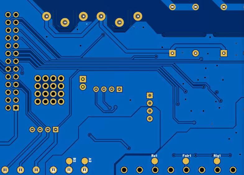
Depth tolerance governs how accurately a manufacturing process can control the vertical dimension of a feature—whether it is a drilled via, laser microvia, backdrilled stub, cavity, or embedded structure. Unlike lateral tolerances, which are often visible and easier to measure, depth-related deviations are hidden within the board stack-up. This invisibility is precisely what makes depth tolerance so dangerous when poorly controlled.
From my perspective, depth tolerance represents a silent boundary between functional success and latent failure. Many electrical, mechanical, and thermal problems observed in the field do not originate from design mistakes, but from accumulated depth inaccuracies during fabrication.

Depth tolerance
Depth-tolerance refers to the allowable deviation between the intended depth of a manufactured PCB feature and its actual achieved depth. This applies to vertical structures such as drilled holes, laser vias, controlled-depth milling, backdrilling, countersinks, cavities, and embedded component recesses.
In multilayer PCBs, depth tolerance is not a single value but a compound result influenced by:
Material thickness variation
Lamination flow and resin distribution
Drill and laser calibration accuracy
Tool wear and machine rigidity
Registration alignment across layers
Unlike width or diameter tolerances, depth-tolerance directly affects layer-to-layer connectivity. A via that stops 20 microns too short may fail electrically; one that goes 20 microns too deep may damage an adjacent plane or compromise impedance.
In my experience, depth tolerance is best understood not as a mechanical limit, but as a process capability indicator. When depth tolerance control is poor, it signals instability in upstream lamination, drilling, or thickness control—issues that will eventually surface as yield loss or field failures.
Multilayer PCBs rely on precise vertical alignment between conductive layers. Depth tolerance determines whether vias land exactly where the designer intended within the Z-axis of the stack-up.
In high-layer-count boards, even small depth errors can cascade:
Over-drilling can thin internal copper planes
Under-drilling can leave incomplete interconnections
Inconsistent depths can cause impedance variation across identical nets
What makes depth tolerance especially critical is that vertical errors are cumulative. Each lamination cycle introduces thickness variability, and each subsequent drilling or laser process must compensate for those variations.
From a manufacturing viewpoint, depth tolerance control is essentially stack-up discipline translated into execution. Without tight vertical control, even the most carefully designed multilayer architecture becomes vulnerable.
Mechanical drilling remains widely used for through-holes and larger vias. In this process, depth tolerance is influenced by:
Drill bit length accuracy
Z-axis positioning repeatability
Entry and backup material compression
Panel flatness
Mechanical drills do not “sense” internal layers. They rely entirely on programmed depth values, assuming that the stack thickness matches the nominal design. When that assumption fails, depth tolerance errors appear.
In practical production, I have observed that manufacturers who treat drilling depth as a fixed parameter often struggle with yield consistency. In contrast, those who actively measure post-lamination thickness and dynamically adjust drilling depth maintain tighter depth tolerance and more reliable interconnections.
Laser drilling introduces a different depth-tolerance challenge. Instead of physical contact, material removal depends on energy absorption, pulse duration, and dielectric composition.
Laser depth-tolerance is affected by:
Resin glass content variation
Copper reflectivity differences
Laser focus drift
Heat accumulation during high-density drilling
Unlike mechanical drilling, laser processes can partially self-limit when encountering copper layers. However, this does not eliminate depth tolerance concerns—it simply changes their nature. Over-ablation can damage capture pads, while under-ablation can leave resin residues that compromise plating adhesion.
In my view, laser depth tolerance is a test of process intelligence rather than brute precision. Advanced manufacturers use feedback systems, test coupons, and adaptive laser parameters to maintain consistent depth outcomes.
When depth tolerance is properly controlled, several key advantages emerge:
Improved Interconnect Reliability
Consistent via depths ensure complete electrical connections without over-stressing adjacent layers.
Higher Yield Stability
Tight depth tolerance reduces rework, scrap, and latent defects that appear only after thermal cycling.
Enhanced Signal Integrity
Uniform vertical structures reduce impedance variation and reflection points.
Better Compatibility with Advanced Designs
HDI, backdrilled, and embedded structures all depend on predictable depth control.
Manufacturers with mature depth tolerance management—such as JM PCB, which integrates thickness measurement and depth compensation into its fabrication workflow—tend to deliver boards with noticeably higher consistency across production lots.
Depth tolerance has a direct and indirect influence on electrical behavior.
Direct impacts include:
Incomplete vias increasing resistance
Over-drilled structures creating parasitic capacitance
Backdrill depth errors leaving signal stubs
Indirect impacts include:
Increased impedance discontinuities
Higher insertion loss in high-speed channels
Reduced signal eye opening
From a signal integrity standpoint, depth tolerance is inseparable from performance predictability. A design that simulates perfectly on paper can fail in reality if vertical dimensions drift beyond acceptable limits.
Backdrilling is one of the most depth-sensitive processes in modern PCB manufacturing. Its purpose is simple in concept—remove unused via stubs—but extremely unforgiving in execution.
Depth tolerance in backdrilling defines the boundary between success and failure:
If the drill stops too early, residual stubs remain and degrade signal integrity.
If it drills too deep, it risks severing the functional via connection.
In multilayer boards operating at high frequencies, even a residual stub of tens of microns can introduce reflections, impedance discontinuities, and increased insertion loss. This makes depth tolerance not just a mechanical concern, but a high-speed electrical requirement.
From my observation, backdrilling exposes a fundamental truth: depth tolerance cannot be treated as a static number. It must be dynamically adjusted based on:
Actual laminated thickness
Copper distribution across layers
Local board warpage
Factories that rely solely on nominal stack-up values often experience inconsistent backdrill performance, even when using advanced drilling equipment.
| Benefit Category | Depth Tolerance Contribution |
|---|---|
| Electrical Reliability | Ensures complete via connections and stable impedance profiles |
| Signal Integrity | Minimizes residual stubs and vertical impedance discontinuities |
| Mechanical Strength | Reduces stress concentration at via-to-pad interfaces |
| Thermal Performance | Maintains consistent thermal via depth for heat dissipation |
| Yield Stability | Lowers scrap and rework caused by drilling depth errors |
| Lifecycle Reliability | Reduces latent failures after thermal cycling and aging |
As multilayer PCB structures continue to grow in complexity, it becomes increasingly clear that reliability is no longer determined solely by materials, trace geometry, or layer count. Instead, it is shaped by how precisely manufacturers can control what is often invisible—the vertical dimension.
Depth tolerance sits at the heart of this challenge. It governs whether interconnects reach their intended targets, whether signal paths remain electrically clean, and whether mechanical and thermal stresses are evenly distributed throughout the board. When depth tolerance is well managed, multilayer interconnects behave predictably across temperature, time, and operating conditions. When it is neglected, even the most advanced designs are exposed to hidden vulnerabilities.
From my perspective, depth tolerance is not merely a specification on a drawing. It is a reflection of manufacturing philosophy. Companies that treat depth control as a secondary concern often struggle with yield instability and latent failures. Those that elevate depth tolerance to a core process discipline consistently deliver boards that perform as designed—not only at test, but throughout their service life.
In the end, depth tolerance represents a quiet but decisive form of engineering control. It does not attract attention when done well, yet its absence is unmistakable when failures emerge. For reliable multilayer interconnects, mastering depth tolerance is no longer optional—it is essential.
Not necessarily. While tighter control may require better equipment and process discipline, it often reduces overall cost by improving yield, minimizing rework, and preventing costly field failures. In many cases, good depth tolerance control lowers total lifecycle cost.
Depth-tolerance directly influences via stub length, interlayer connectivity, and impedance continuity. Poor depth control can leave residual stubs or over-drilled structures, leading to signal reflections, increased insertion loss, and degraded eye diagrams in high-speed designs.
Yes. HDI boards rely heavily on microvias, stacked vias, and sequential lamination. These structures are highly sensitive to vertical inaccuracies, making depth-tolerance far more critical than in traditional through-hole designs.
Not always. Many depth tolerance defects do not cause immediate electrical failures. Instead, they manifest over time as reliability issues such as intermittent opens, increased resistance, or failures after thermal cycling.
Depth-tolerance is controlled through a combination of accurate stack-up modeling, post-lamination thickness measurement, calibrated drilling or laser systems, and feedback loops that adjust process parameters based on real production data.


Connect to a Jerico Multilayer PCB engineer to support your project!
Request A Quote


 Quote
Quote