


+86 13603063656
Printed Circuit Board (PCB) design has always balanced electrical performance, manufacturability, and mechanical constraints. As devices shrink and the demand for more integrated features grows, the role of mechanical features on PCBs becomes increasingly critical. Among these features, PCB slotting stands out as one of the most effective methods to manage space, improve mounting flexibility, and enhance the mechanical interface between a board and its components.
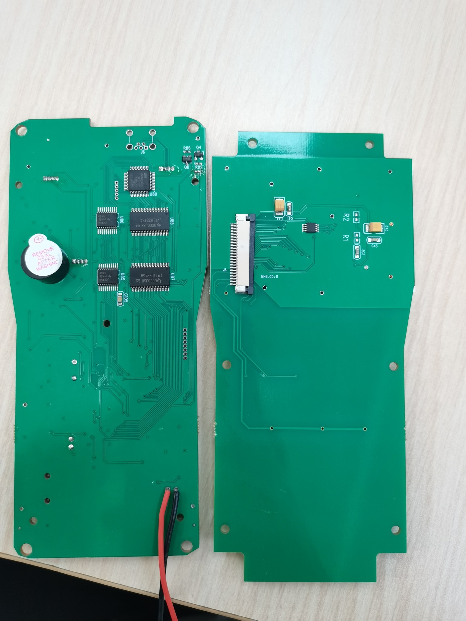
PCB slotting refers to creating precisely defined elongated cutouts or channels in a PCB. Unlike simple drilled holes, slots can provide large or irregularly shaped openings that support connectors, alignment pins, mounting screws, and even airflow channels. Designers use slotting to solve a range of challenges, from enabling unique component form factors to improving board rigidity by managing stress paths.
In today’s electronics, PCB slotting is not just a convenience—it’s often a necessity. Designers in automotive, aerospace, medical devices, and high-density consumer electronics rely on slotting to reduce footprint, improve mechanical fit, and increase reliability. With miniaturization trends and 3D integration continuing to rise, the importance of mastering PCB slotting cannot be overstated.

PCB slotting
From years of working on mixed-signal boards and ruggedized embedded systems, I’ve seen firsthand how poorly planned slots can lead to mechanical failure, electromagnetic interference, or even total board rejection during assembly. Conversely, well-executed slotting can transform a board from a “problem child” into a production-ready, highly reliable design. In my view, the true value of PCB slotting lies not just in the physical space it creates but in the design discipline it enforces: thinking holistically about the mechanical, thermal, and electrical roles a board plays in the system.
This is why in this guide, I’ll cover not only the technical details but also the decision-making frameworks that help designers know when, where, and how to apply PCB slotting effectively.
At its simplest, PCB slotting involves using either mechanical routing or laser cutting to remove portions of the PCB substrate in non-round shapes. While plated through-holes remain the standard for component leads and vias, slots allow for:
Mounting tabs of power transistors or connectors
Air gaps for isolation in high-voltage designs
Clearance for odd-shaped components or assemblies
Stress relief between zones of differing thickness
Fabrication methods:
Mechanical Routing: Using a small-diameter end mill to cut slots with high precision. This is the most common method and suits FR-4 boards.
Laser Cutting: Ideal for very thin boards or flexible substrates, providing higher precision and smaller radii.
Punching or Stamping: Used in high-volume production for standardized slot geometries.
Plated vs. Non-Plated Slots:
Plated Slots are lined with copper and typically used when component leads or pins pass through, providing both electrical and mechanical connection.
Non-Plated Slots serve purely mechanical purposes, like mounting or alignment.
PCB slotting offers multiple advantages when implemented correctly:
Space Optimization: Allows components with unusual footprints or mounting tabs to be embedded without increasing board outline size.
Improved Mechanical Mounting: Enables secure placement of connectors, heatsinks, or structural support elements.
Electrical Isolation: Slots can create air gaps to meet creepage and clearance requirements, especially important in power and high-voltage systems.
Thermal Pathways: Slots improve airflow and can help dissipate heat around high-power components.
Flexibility in Assembly: Supports modular assembly, alignment pins, or snap-fit structures.
Despite its advantages, PCB slotting brings a host of design and manufacturing challenges:
Tolerance Control: Slots must be tightly controlled for width and position to ensure component fit.
Mechanical Weakening: Large or poorly placed slots can compromise board rigidity.
Stress Concentration: Sharp corners can create crack initiation points, especially during thermal cycling.
Cost Increase: Complex slotting patterns can increase routing time and manufacturing costs.
Approaches to Solving Challenges:
Use Rounded Ends: Always specify a radius at slot ends to reduce stress concentration.
Panelization Planning: Ensure slots don’t interfere with depanelization tools or break-away tabs.
Pre-Manufacturing Reviews: Work closely with your PCB vendor to check slot tolerances before committing to production.
Material Selection: For high-stress environments, choose substrates with higher flexural strength.
Finite Element Analysis (FEA): For critical applications, simulate stress distribution to predict weak points.
As electronic systems become smaller and more complex, PCB slotting plays an increasingly pivotal role in meeting both spatial and mechanical constraints. Engineers designing compact products—wearables, medical instruments, industrial controls—often discover that traditional drill holes or larger board outlines simply cannot accommodate the required connectors, components, and mechanical interfaces. PCB slotting emerges as a powerful tool to address these constraints without inflating board size or cost.
The continued drive toward miniaturization puts enormous pressure on PCBs to do more with less. Traditional round vias or large copper keep-outs are insufficient when:
Components have non-standard footprints or mounting tabs.
High-current traces require thicker copper and unique thermal dissipation features.
Multiple boards must interlock mechanically in a small enclosure.
By using PCB slotting, designers create elongated cutouts or channels to guide connectors, facilitate press-fit tabs, or allow airflow without increasing the overall board footprint. This practice directly translates into smaller and lighter devices.
A crucial but sometimes overlooked function of PCB slotting is its ability to mechanically integrate a PCB into the larger assembly. Think of it as creating an “anchor point” or “alignment rail” right inside the board. Examples include:
Snap-Fit Features: Using slots to anchor snap-fit plastic housings without additional screws.
Alignment Keys: Ensuring connectors or daughterboards seat in exactly the right orientation.
Stress Relief: Allowing different zones of a board to flex or thermally expand without cracking.
This mechanical integration allows designers to eliminate separate brackets or fasteners, thereby reducing part count and assembly time.
PCB slotting is also invaluable for thermal management. In high-power designs, components like MOSFETs or power regulators generate heat that must be dissipated. Slots allow air to flow through or around hot spots, reducing temperature gradients. They also make it easier to insert heatsinks or metal backplates directly through the board.
By enabling better airflow, PCB slotting can reduce the reliance on bulky fans or heat spreaders, which in turn supports miniaturization and reliability goals.
Another application area is high-voltage isolation. Slots are widely used to increase the creepage and clearance distances between conductors on a PCB. This is particularly important in power supplies, automotive electronics, or any design subject to safety standards like UL, IEC, or ISO. Slots cut directly in the dielectric material provide a physical barrier to arcing, thus improving safety and compliance.
Designing with PCB slotting is not simply a matter of drawing cutouts. Dimensions, placement, and interface details all influence manufacturability and performance. This section provides a framework for designers to follow.
Slot dimensions affect manufacturability, component fit, and board strength. Some best practices:
Width Tolerance: Match slot width to the component pin or tab plus a small clearance (e.g., 0.1–0.2 mm) to account for manufacturing variance.
Length Allowance: Provide at least 0.3–0.5 mm longer than the component’s mounting tab to ease insertion.
End Radius: Include a radius at each end of the slot equal to the router bit radius or larger to reduce stress concentrations.
Where you place a slot on the board matters. Consider:
Distance from Edge: Keep at least 1 mm from the board edge for structural integrity unless intentionally creating a breakaway tab.
Avoiding High-Stress Zones: Do not place slots too close to screw holes, large BGAs, or regions subject to repeated flexing.
Panelization Considerations: Ensure slots do not interfere with fiducials or depanelization tooling.
PCB slotting can become the bridge between PCB and enclosure. For example:
Mounting Screws and Standoffs: Use slots to allow for slight tolerance mismatches during assembly.
Floating Connectors: Give connectors some mechanical play to absorb stress without cracking solder joints.
Structural Braces: Design slots to accept metal or composite stiffeners that run through the board for added rigidity.
Always weigh the electrical impact of slotting against the mechanical benefit:
Trace Routing: Avoid cutting off return paths or introducing impedance discontinuities.
EMI Concerns: Large slots may affect ground plane continuity and increase radiated emissions.
Thermal Relief: Use copper pours and thermal vias to manage heat around slotted areas.
Material selection underpins the success of any PCB slotting strategy. Certain substrates and copper foil types handle slotting better than others.
Common FR-4 substrates are versatile but can become brittle if slotting is too aggressive. For high-stress or high-temperature environments, consider:
Polyimide: For flexible or high-temperature applications.
Metal Core PCBs: For thermal management but require specialized routing.
High-Tg FR-4: Offers better mechanical stability and heat resistance.
Different copper foil types affect how the plated area around a slot behaves.
Rolled Copper Foil: Mechanically rolled to produce a smoother, denser copper with excellent ductility.
Electrolytic Copper Foil: Deposited electrolytically, offering cost-effectiveness and good flexibility.
(We’ll revisit this distinction in the FAQ section as one of the requested entries.)
When you know a slot will experience repeated stress (e.g., insertion/removal of connectors), reinforce the area:
Add extra copper pads or thicker plating along slot walls.
Use stiffener materials bonded to the PCB backside.
Design interlocks so forces are transferred to the enclosure rather than the board.
Be aware that exotic materials or very thin copper can complicate slotting. Work with your manufacturer to find a compromise between performance and cost. JM PCB, for instance, offers DFM (Design for Manufacturability) reviews that specifically highlight slotting challenges and suggest alternative stack-ups—something I’ve found invaluable when pushing design limits.
High-density boards bring together tight component spacing, fine-pitch BGAs, and strict impedance requirements. Introducing PCB slotting into this environment can solve space issues but also introduce significant risks if not carefully engineered.
As designers push for more functionality in less area, the paradox emerges: adding slots creates space but also removes structural material. In HDI (High Density Interconnect) boards, every square millimeter counts, and cutouts can drastically influence stiffness, warpage, and crosstalk.
Slots can act as unintended discontinuities in the ground or power planes. If a critical differential pair crosses a slotted region, impedance mismatches and increased EMI can occur. To mitigate this:
Route Around Slots: Keep high-speed signals at least 2–3 mm from slot edges.
Stitch Ground Vias: Provide return paths on either side of a slot to preserve plane continuity.
Use Guard Traces: For sensitive analog circuits near slotted areas.
When boards are densely populated, rework or field service often requires mechanical handling. Slots can make a board more fragile during this handling, especially if large cutouts intersect stress-prone areas. Designers should:
Add keep-out zones around slots for critical components.
Consider stiffener plates or “dogbone” shaped copper reinforcements near slot perimeters.
Use progressive slotting (several smaller slots rather than one big slot) to preserve rigidity.
Because HDI designs often carry high currents or pack heat-generating components, slotting can improve airflow but also reduce copper area for heat spreading. Balance is key. Evaluate whether a slot’s thermal advantage outweighs its loss of copper conduction.
Once a slot is introduced into a PCB, you’re essentially creating a mechanical notch. Notches concentrate stress and can become crack initiation points. This section dives into the mechanical reliability aspect of PCB slotting.
Any time you remove material from a load-bearing surface, stress concentrates at the boundaries. The sharper the boundary, the higher the stress. PCBs are no exception:
Sharp Corners create high stress risers.
Thin Bridges between slots and board edges are prone to cracking.
Differential Expansion between copper and substrate amplifies stress at plated slot edges.
Best practices for reducing mechanical risk:
Use Rounded Ends: Match the router bit radius or specify larger arcs.
Maintain Minimum Web Width: Keep at least 1.5 mm of material between adjacent slots or between a slot and the board edge whenever possible.
Align Slots With Stress Direction: Place slots parallel to expected bending or force vectors rather than perpendicular.
Choose substrates with higher flexural strength if your board will experience vibration or bending. High-Tg FR-4 or polyimide layers can help. Also consider thicker copper plating or metal stiffeners at critical slots.
Plated slots can add mechanical strength because the copper lining acts like a reinforcement sleeve. However, plating introduces its own stress due to different thermal expansion rates. Decide based on whether the slot will carry electrical current or purely mechanical loads.
It’s essential to validate slotting choices with testing:
Vibration Testing: To simulate shipping or automotive environments.
Thermal Cycling: Repeated heating and cooling can reveal crack initiation points.
Insertion/Extraction Cycles: If a component pin slides through a slot, test its life cycle.
One of the most important yet underestimated functions of PCB Slotting is its effect on heat dissipation and signal behavior. When designed correctly, slots can be a powerful ally for both thermal management and maintaining signal integrity.
Slots act as “micro-vents” within the PCB. This is especially valuable in high-power boards, LED drivers, or motor controllers. Properly placed PCB Slotting allows:
Direct airflow over heat-sensitive components.
Reduced hot spots on copper pours.
Integration of small heatsinks through the board itself.
Designers should model airflow early on. Computational Fluid Dynamics (CFD) tools can simulate how air moves through and around slots, allowing you to place them where they’ll have the greatest cooling impact.
Sometimes you don’t want heat to spread. In high-precision analog or RF sections, a slot can act as a thermal moat, isolating heat-generating areas from sensitive circuits. This maintains signal stability and reduces drift.
Key tactics:
Add slots between high-power and low-power sections.
Use narrow but continuous slots to “cut off” thermal conduction paths.
Combine slotting with thermal vias or copper pours to channel heat precisely.
Although slots can improve thermal performance, they can disrupt current return paths or ground planes. For high-speed digital or RF signals, improper slotting may lead to impedance discontinuities, reflections, and emissions.
To mitigate:
Avoid routing high-speed traces across slots.
Stitch ground vias tightly around slots to maintain reference planes.
Use copper “bridges” or buried ground planes beneath slotted areas if stack-up allows.
Beyond thermal and electrical benefits, PCB Slotting is a cornerstone of mechanical assembly. Well-planned slots can reduce assembly time, improve alignment, and increase product robustness.
Slots help guide components or modules into their correct positions during assembly. For example:
Connector Tabs: Align large connectors without extra jigs.
Board-to-Board Interconnects: Guide daughtercards into backplanes.
Sensors and Displays: Precisely position fragile parts to avoid stress.
Designers should work from the mechanical drawing backwards, ensuring slot dimensions match real-world tolerances of mating parts.
Slots are widely used for screws, standoffs, and snap-fit clips. Tips for success:
Elongated slots allow slight tolerance mismatch in enclosure screw bosses.
Plated slots provide stronger anchor points for press-fit pins.
Reinforced copper pads around slot edges improve torque resistance.
In automated assembly, slots can double as pick-and-place fiducials or as references for robotic arms. However, if slots are too thin or irregular, vacuum nozzles may fail to hold the board. Coordinate with your assembly house to ensure slot geometry supports automated handling.
By designing slots to perform multiple roles — alignment, anchoring, thermal relief — you reduce the need for extra brackets or fasteners. This can lower BOM costs and simplify your supply chain.
Flexible and rigid-flex PCBs add an entirely new dimension to board design. Integrating PCB Slotting into these formats requires extra care because the materials behave differently than standard FR-4.
Flex substrates such as polyimide are much thinner and more pliable than rigid boards. When introducing slots:
Stress Distribution: Slots can act as stress concentrators during bending.
Tear Propagation: In flex areas, a slot can become the origin of a crack if not properly reinforced.
Plating Complexity: Plated slots in flexible materials require specialized processes to avoid delamination.
Key methods to reinforce flex boards with slots:
Stiffener Layers: Bonded polyimide or FR-4 stiffeners over slotted regions.
Adhesive Fillets: Applying additional adhesive around slot edges to resist peel forces.
Copper Tie-Bars: Small copper traces across slots to keep alignment until after assembly.
The junction between rigid and flexible sections is a natural stress point. When placing slots near these transitions:
Maintain a generous transition radius.
Avoid overlapping slot ends with plated through-holes.
Simulate bend cycles to ensure long-term durability.
Designers often underestimate how much PCB Slotting influences fabrication cost and yield. Because slotting removes material and requires special routing or laser operations, even small changes to tolerances or geometry can ripple into cost overruns.
Every slot has a width and length tolerance. Combined with the tolerances of component tabs, this creates a stack-up that must be managed. If your slot is too narrow, assembly fails; too wide, and mechanical stability suffers.
Tips:
Work with ±0.1 mm as a realistic router tolerance for many FR-4 boards.
Provide your fabricator a full mechanical drawing of slot geometry.
Request “go/no-go” gauges during prototype builds to verify fit.
Routing: Less expensive for larger slots but limited by router bit size.
Laser Cutting: Higher precision and tighter radii, but costlier and slower at volume.
Designers should match slot requirements to the process that balances precision and budget.
Slots can interfere with panel rails, tooling holes, or break-away tabs. Always consider:
Adding sacrificial “bridges” around slots to maintain panel rigidity.
Aligning slot orientation with depanelization tooling to reduce stress.
Using test coupons to measure slot consistency across the panel.
Combine multiple small slots into a single routed operation.
Standardize slot sizes where possible to reduce tool changes.
Place slots away from copper-dense areas to minimize scrap.
Even the best design for PCB Slotting can underperform if not validated properly. Testing confirms that mechanical, electrical, and environmental performance meet specifications before mass production.
Testing methods:
Push/Pull Tests: Measure how much force is needed to dislodge components held by slotted regions.
Fatigue and Vibration: Apply cyclic bending or vibration to see if cracks develop at slot edges.
Drop Testing: Simulate accidental drops to evaluate mechanical integrity.
Because PCBs experience temperature swings, thermal cycling checks:
CTE Mismatch between slot walls and adjacent copper.
Delamination Risk around plated slots.
Creep of Adhesive Layers in rigid-flex designs.
Slots can affect return paths and EMI shielding. Validation steps:
Measure impedance before and after slot integration.
Use time-domain reflectometry to detect discontinuities.
Check for increased crosstalk in high-speed traces adjacent to slots.
If the product faces moisture, dust, or chemical exposure, test:
Conformal coating adhesion near slots.
Water ingress along slot edges.
Corrosion at exposed copper in plated slots.
This section wraps up the article and answers key questions designers often have about PCB Slotting.
Miniaturization Pressure: Slots will become narrower, requiring laser or micro-milling.
Hybrid Boards: Rigid-flex and embedded components will demand advanced slotting.
AI-Assisted DFM: Software tools will automatically optimize slot placement for strength and EMI.
New Materials: Copper-aluminum hybrid boards and advanced polyimide will improve reliability.
When implementing complex slotting or high-volume production, partnering with JM PCB provides consistent quality, competitive pricing, and tailored engineering support. I believe designers will soon treat slotting as a “first-class design feature” rather than a last-minute mechanical cut. This mindset shift can unlock better reliability and lower costs. “PCB Slotting” is no longer just a mechanical afterthought. It’s a deliberate, strategic design choice enabling compact layouts, secure mounting, and improved performance. By following the practices discussed — and working with experienced manufacturers like JM PCB — designers can confidently solve space and mounting challenges.
FAQ 1: What is the difference between rolled copper foil and electrolytic copper foil?
Rolled copper foil is produced by mechanically rolling copper into thin sheets, offering better surface quality and mechanical strength. Electrolytic copper foil is deposited via an electrolytic process and is more flexible and cost-effective.
FAQ 2: How does PCB Slotting affect signal integrity?
Slots can disrupt return paths and increase EMI. Placing ground stitching vias around slots or adding copper pours can mitigate this effect.
FAQ 3: What is the typical manufacturing tolerance for PCB Slotting?
Routed slots usually have ±0.1 mm tolerance, while laser-cut slots can achieve ±0.05 mm. Discuss tolerances with your PCB house early to avoid surprises.
FAQ 4: Are plated slots always better than non-plated slots?
Not necessarily. Plated slots are great for mechanical strength and electrical continuity, but they cost more and have tighter manufacturing constraints. Non-plated slots are simpler for isolation or relief.
FAQ 5: Can PCB Slotting improve thermal management?
Yes. Designers often use slots to create airflow channels or isolate hot zones from cold zones, reducing thermal stress on critical components.


Connect to a Jerico Multilayer PCB engineer to support your project!
Request A Quote


 Quote
Quote