


+86 13603063656
Signal integrity is one of the most critical challenges in modern RF design. As devices continue to operate at higher frequencies and tighter tolerances, the pathway through which signals travel—the printed circuit board (PCB)—becomes increasingly important.
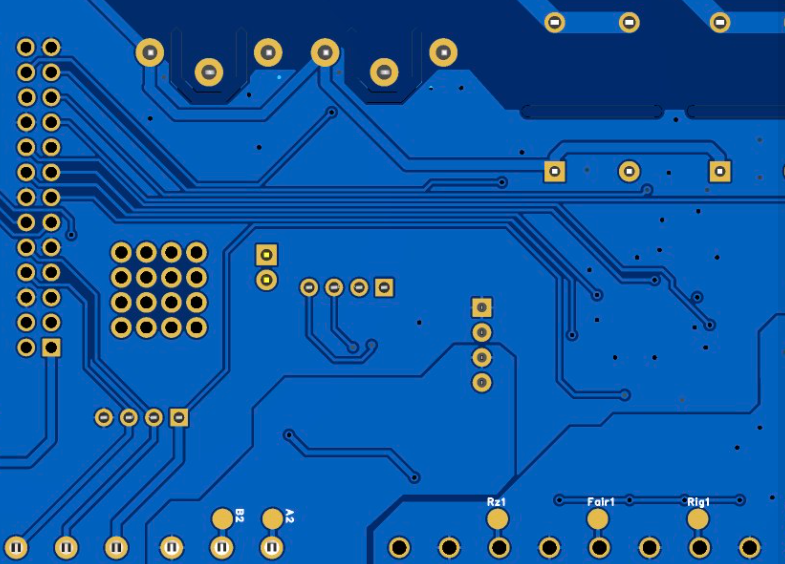
PCB Routing is the art and science of guiding electrical signals along controlled paths while minimizing losses, interference, and distortions. In RF systems, where wavelengths may be comparable to trace lengths, small deviations in routing can cause dramatic effects such as impedance mismatches, reflections, and crosstalk.
In this article, I will provide not just a detailed technical guide, but also my reflections on why precision in PCB Routing is more than a design step—it is a fundamental enabler of reliability and performance in RF electronics.

PCB Routing
At its core, PCB Routing involves the process of creating copper pathways on a printed circuit board to connect components while adhering to strict electrical and mechanical constraints. Unlike low-frequency designs, where routing is largely about physical connectivity, RF routing requires engineers to treat traces as transmission lines.
Some fundamentals include:
Controlled Impedance: Every PCB trace at RF acts as a transmission line. Designers must calculate and maintain consistent impedance values, usually 50Ω or 75Ω.
Length Matching: Signal delays are directly proportional to trace length. In differential pairs, mismatches can introduce skew and degrade performance.
Return Path Integrity: Proper ground referencing ensures current returns via the lowest inductance path, reducing EMI and ensuring stable operation.
Crosstalk Control: Careful spacing and shielding minimize coupling between adjacent traces.
From my perspective, the biggest challenge is balancing theoretical design rules with practical board layout constraints. Engineers often face trade-offs between ideal RF routing and component density. The ability to prioritize signal-critical nets during PCB Routing is a mark of design expertise.
A well-executed PCB Routing strategy provides significant benefits:
Preservation of Signal Integrity – By controlling impedance and minimizing reflections, the original waveform is transmitted with minimal distortion.
Improved Reliability – Stable routing ensures consistent performance across temperature, humidity, and aging factors.
Lower Electromagnetic Interference (EMI) – Correct return paths and shielding reduce emissions, ensuring compliance with regulatory standards.
Optimized Power Efficiency – Lower losses mean reduced power consumption in RF front-ends and transmission lines.
Design Scalability – Well-documented routing rules simplify future iterations or redesigns.
From a personal standpoint, one overlooked benefit of proper PCB Routing is manufacturability. A design that follows clear routing principles is easier for manufacturers to produce consistently. This is why partnering with reliable PCB suppliers like JM PCB can make a difference—they not only fabricate but also provide design-for-manufacturing insights that protect signal integrity in real-world production.
The PCB Routing process can be divided into several stages:
Schematic Capture: Defining connections and design intent.
Component Placement: Strategic positioning to minimize routing complexity and critical path lengths.
Routing Strategy Definition: Deciding on controlled impedance traces, differential pairs, via management, and signal prioritization.
Execution of Routing: Laying copper paths in CAD tools, adhering to design rules, and ensuring DRC (Design Rule Check) compliance.
Signal Integrity Analysis: Running simulations to confirm impedance, timing, and crosstalk compliance.
Fabrication Considerations: Ensuring trace widths, clearances, and stack-up match manufacturer capabilities.
Prototype Testing: Verifying with TDR (Time Domain Reflectometry), VNA (Vector Network Analyzer), and EMI compliance tests.
What I find fascinating is how much iteration happens in this process. Rarely does a perfect layout emerge in the first attempt. Instead, RF designers loop through simulations, adjustments, and reviews until the PCB Routing achieves balance between theory and manufacturability.
When engineers discuss PCB Routing, the conversation often shifts quickly toward design considerations. This is because routing is not simply a matter of connecting two pads with a copper trace; rather, it is an optimization process balancing electromagnetic theory, practical design constraints, and manufacturability.
Every high-frequency trace is essentially a transmission line, and impedance mismatches cause reflections that degrade signal integrity. Therefore, one of the foremost considerations in PCB Routing is maintaining controlled impedance.
Trace Geometry: Width, spacing, and thickness directly impact impedance.
Dielectric Material: The dielectric constant (Dk) of the PCB substrate affects signal velocity and impedance.
Stack-up Design: Consistent layer spacing ensures predictable impedance across the board.
In my experience, early collaboration with a PCB manufacturer to validate achievable trace widths and dielectric properties avoids costly redesigns. For instance, working with a vendor like JM PCB can provide confidence that the chosen stack-up supports both electrical and mechanical requirements.
Crosstalk occurs when signals on adjacent traces couple electromagnetically. In PCB Routing, the following measures help reduce it:
Maintain sufficient spacing between high-speed nets.
Use differential pairs with tight coupling to reject common-mode noise.
Insert ground shielding traces where necessary.
Reflecting on real-world cases, I’ve noticed that designers sometimes prioritize density over spacing, leading to unexpected crosstalk in prototypes. A disciplined approach to spacing is non-negotiable in RF applications.
For every high-speed signal, the return current follows the path of least inductance, usually directly beneath the trace. Interruptions in the ground plane (e.g., splits or cutouts) can force return currents into detours, increasing loop area and EMI. Thus, in PCB Routing, continuous reference planes are vital.
This is one area where design intent often clashes with board real estate. Personally, I think one of the best investments in design tools is electromagnetic field simulation software that can visualize return paths. It has helped me uncover weak spots in layouts that traditional rule-checkers would miss.
Material choice is often underestimated, yet it directly determines how well PCB Routing preserves signal integrity.
High-frequency signals propagate at different velocities depending on the Dk of the substrate. Materials with stable, low Dk values (like PTFE-based laminates) minimize signal delay and dispersion. Variability in Dk across the board stack-up can create impedance mismatches, so consistent material quality is essential.
Loss tangent describes how much signal energy is absorbed as heat in the dielectric. A high Df means greater signal attenuation. For RF and microwave designs, low-loss materials like Rogers laminates are often chosen to ensure efficient PCB Routing.
I often weigh cost versus performance here. While high-end materials improve performance, they significantly raise costs. I’ve found that working closely with manufacturers allows optimization—for example, using premium materials only for critical RF layers, while standard FR-4 suffices for control circuitry.
Copper type and roughness impact conductor losses. Rolled copper foil provides smoother surfaces and lower insertion loss compared to electrolytic copper foil. This is particularly important for PCB Routing in millimeter-wave frequencies.
Interestingly, I’ve seen projects where a design performed perfectly in simulation but failed in production, simply because the assumed copper roughness didn’t match the manufacturer’s actual material. This reinforces why designers must validate not only geometry but also copper specifications with PCB suppliers.
RF systems often operate in environments with temperature swings. Materials with stable dielectric properties across temperature ranges are crucial. Additionally, mechanical strength ensures that fine traces used in PCB Routing do not deform under stress or vibration.
Once the basics are mastered, engineers move into advanced techniques that push the limits of PCB Routing in RF systems.
Differential signals are routed in pairs to improve noise immunity. For these to work effectively:
Trace lengths must be matched within tight tolerances.
Pair spacing must remain consistent to maintain differential impedance.
Symmetry is critical; asymmetry introduces common-mode noise.
I’ve observed that engineers new to RF often underestimate how strict these tolerances must be. A mismatch of just a few mils can create significant timing skew at gigahertz frequencies.
Vias introduce parasitic inductance and capacitance, which can disrupt signal flow. Advanced PCB Routing minimizes via count on critical RF paths, or uses back-drilling and via stubs removal to reduce reflections.
My reflection here: I believe via usage is one of the most overlooked aspects in RF layouts. Many digital designers route freely with vias, but in RF, each via can act like a discontinuity. Thinking of vias as components, rather than neutral pass-throughs, is a mindset shift crucial for good RF design.
Specialized routing structures like microstrips and coplanar waveguides allow precise impedance control. These are especially important in RF front-ends and antenna feeds.
Microstrip: Signal trace over a reference plane, simple and widely used.
Coplanar Waveguide (CPW): Signal trace flanked by ground traces, improving isolation and impedance control.
Advanced designers often combine these structures within the same board. Personally, I enjoy experimenting with CPW structures in simulations—they offer creative solutions for compact layouts while still ensuring robust performance.
Adding grounded guard traces between sensitive lines reduces coupling. For critical RF paths, entire sections may be shielded using via fences or metal enclosures.
The first time I saw a properly implemented via fence, I was struck by how elegant the solution was. It showed me that PCB Routing is not just about traces—it’s about controlling the entire electromagnetic environment around those traces.
Even experienced engineers encounter challenges in PCB Routing, particularly in RF applications where tiny mistakes can undermine months of careful design. Understanding the most frequent pitfalls—and how to mitigate them—is essential for ensuring robust signal integrity.
One of the most common errors is treating high-frequency traces as simple wires rather than transmission lines. This often leads to impedance mismatches, reflections, and loss of signal fidelity.
Solution: Always calculate trace impedance and verify with simulation tools. Document assumptions about dielectric constant and copper thickness.
I’ve personally seen cases where teams assumed “short traces don’t matter.” At GHz frequencies, even a few millimeters can create resonances, leading to failure during compliance testing. This is a pitfall I always caution new designers against.
Vias introduce parasitic inductance and can create stub effects. When too many vias are placed on critical RF paths, performance degradation is inevitable.
Solution: Minimize via usage or employ back-drilling to remove unused stubs. Treat every via as an electrical component, not just a physical connector.
From my reflection, I’ve come to think of vias as necessary evils—sometimes unavoidable, but always requiring thoughtful management.
Splitting ground planes or allowing return paths to cross plane boundaries forces current into indirect paths, increasing EMI and signal distortion.
Solution: Maintain continuous ground planes under critical signals. Use stitching vias liberally to ensure low-impedance return paths.
In one of my projects, poor ground continuity created a nightmare of emissions issues. After correcting the layout with a continuous reference plane, EMI levels dropped dramatically. This taught me that ground design is often more critical than signal routing itself.
As boards shrink in size, traces are routed closer together, increasing the risk of crosstalk.
Solution: Maintain adequate spacing, use differential pairs, and insert guard traces where feasible.
Here, I believe discipline is key. It’s tempting to push density to meet mechanical constraints, but without respect for crosstalk rules, performance collapses.
Designers sometimes specify trace widths or spacings that exceed the capabilities of their chosen manufacturer. This can lead to uncontrolled impedance or outright production failures.
Solution: Collaborate early with PCB vendors. A manufacturer like JM PCB can provide stack-up libraries and tolerance guidelines that align design intent with manufacturing realities.
Simulation and testing are the final guardians of signal integrity. Without thorough validation, even the most carefully planned PCB Routing can hide weaknesses that surface only in prototypes or, worse, in the field.
Advanced CAD tools allow designers to simulate electromagnetic field behavior directly within the board layout. This ensures:
Controlled impedance validation.
Crosstalk prediction.
Reflection analysis across frequency ranges.
In my experience, simulation bridges the gap between theory and practice. While it cannot capture every nuance of manufacturing variability, it reveals major risks before physical fabrication.
TDR testing is used to verify impedance continuity. A fast rise-time signal is sent through the trace, and reflections are measured. This reveals:
Discontinuities at vias or connectors.
Variations in trace impedance.
Quality of return paths.
I’ve always found TDR fascinating because it visualizes the hidden imperfections inside a board. It feels like peering into the veins of an electronic system.
VNAs measure S-parameters to evaluate how signals propagate through the PCB. For RF designs, S11 (return loss) and S21 (insertion loss) are particularly critical.
High return loss indicates good impedance matching.
Low insertion loss means minimal attenuation.
In practice, VNAs confirm whether theoretical design goals translate into real-world performance. To me, this is the moment of truth for any PCB Routing effort.
For high-speed digital signals, eye diagrams help assess signal quality by overlaying many bit transitions. Jitter, noise, and amplitude margins become visible.
Open eye diagrams = healthy signals.
Closed eyes = timing or interference issues.
I find eye diagrams particularly rewarding because they transform abstract integrity issues into a clear, visual format that anyone—even non-engineers—can understand.
Testing is rarely a one-off process. Results often lead to layout refinements, stack-up adjustments, or material changes. Successful PCB Routing is iterative, not linear.
Throughout this comprehensive exploration, one theme emerges: PCB Routing is both science and art. It requires mastery of electromagnetic theory, deep respect for manufacturing realities, and the creativity to navigate design trade-offs.
From fundamentals like impedance control and crosstalk mitigation to advanced techniques such as differential pair matching and via management, every decision in routing shapes the destiny of the signal. PCB Routing is a humbling discipline. It teaches patience, attention to detail, and respect for physics. There is no room for shortcuts; every trace carries the weight of performance, reliability, and compliance.
Looking ahead, the challenges of miniaturization, higher frequencies, and emerging materials will push designers further. Yet, I believe the combination of human expertise, automation, and strong partnerships will ensure that signal integrity is not only preserved but enhanced.
In the end, precision in PCB Routing is not optional—it is the foundation of trust in every RF system.
Rolled copper foil is produced by mechanically rolling copper into thin sheets, offering smoother surfaces, better mechanical strength, and lower insertion loss at high frequencies. Electrolytic copper foil is deposited via an electrolytic process, making it more flexible and cost-effective but slightly rougher in surface texture.
Impedance control ensures that signals travel without reflections or losses. In RF systems, mismatched impedance causes return loss, degraded signal quality, and increased EMI emissions. Controlled impedance is therefore central to successful PCB Routing.
At high frequencies, signals travel along the surface of copper (skin effect). Rough copper increases resistance and insertion loss. Choosing smoother copper types, like rolled copper, improves high-frequency performance in PCB Routing.
A continuous ground plane provides a stable return path for signals. Interruptions in the plane can force currents into detours, increasing EMI and crosstalk. For effective PCB Routing, always maintain uninterrupted reference planes under high-speed traces.
As devices shrink, routing density increases. This raises risks of crosstalk, EMI, and impedance variation. To address this, engineers use advanced techniques like via-in-pad, differential pairs, and ground fences to preserve signal integrity in miniaturized layouts.


Connect to a Jerico Multilayer PCB engineer to support your project!
Request A Quote


 Quote
Quote