


+86 13603063656
To comprehend the pivotal role of Nickel Plating in PCB reliability, we must first define what it truly is and how it functions within the manufacturing ecosystem. Nickel Plating refers to the controlled deposition of a nickel layer onto the surface of copper pads or traces on a printed circuit board. This deposition may be achieved through either electrolytic plating or electroless plating, depending on design requirements and surface finish selection.
Electrolytic Nickel Plating involves applying an external electric current through a solution containing nickel salts. The PCB serves as the cathode, attracting nickel ions that reduce and form a metallic coating. This process allows for higher deposition rates and control over plating thickness but requires a conductive path and uniform current distribution — challenges that become complex in high-density designs.
Electroless Nickel Plating, on the other hand, relies on an autocatalytic chemical reaction. No external current is applied. Instead, a reducing agent (often sodium hypophosphite) facilitates the nickel ion reduction on catalytic surfaces. This approach ensures excellent uniformity even on non-conductive or irregular geometries and forms the foundation of well-known finishes such as ENIG (Electroless Nickel Immersion Gold) and ENEPIG (Electroless Nickel Electroless Palladium Immersion Gold).
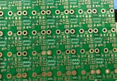
The resulting nickel layer typically measures between 3 to 6 micrometers for ENIG and may reach up to 10 micrometers or more for specific applications requiring enhanced wear resistance. Its primary function is to act as a diffusion barrier between the copper base and the top metal finish. Without this barrier, copper atoms can migrate upward, leading to tarnishing, intermetallic growth, and eventual degradation of solder joints. Nickel Plating thus ensures stable solderability and corrosion resistance while maintaining surface flatness for component mounting.
Beyond its barrier role, Nickel Plating also contributes mechanical strength. Nickel’s inherent hardness enhances resistance to abrasion and contact wear, which is particularly critical in connector pads and edge contacts. In high-cycle environments such as aerospace or industrial control systems, where connectors are mated and unmated thousands of times, the presence of a robust nickel underlayer is the difference between lasting performance and early failure.
From a microstructural standpoint, the integrity of the Nickel Plating layer depends heavily on its crystal structure and phosphorus content (in the case of electroless nickel). High-phosphorus nickel provides better corrosion resistance but slightly lower hardness, while low-phosphorus nickel offers greater wear resistance at the expense of chemical stability. Engineers must choose between these trade-offs depending on the intended operating conditions of the PCB.
The deposition process itself is far from trivial. Factors such as pH level, bath agitation, temperature control, and contamination management all influence the final coating quality. For example, excessive bath decomposition can lead to “black nickel” defects, while poor agitation may cause nodular buildup or uneven thickness. Each defect has downstream implications for solderability, electrical conductivity, and even appearance. Thus, the science of Nickel Plating lies in precision control — in turning chemical chaos into a repeatable metallurgical structure.
The reliability of Nickel Plating becomes evident when viewed through the lens of long-term performance. In accelerated life testing (ALT) environments — including thermal shock, humidity aging, and salt spray exposure — PCBs with properly deposited nickel layers consistently outperform those without. The nickel barrier prevents copper oxidation, limits diffusion, and provides a stable interface for gold or solder. As a result, signal transmission remains stable, contact resistance stays low, and overall board life extends significantly.
In a world increasingly dominated by miniaturization and high-frequency designs, surface finish quality determines success. At microwave frequencies, even minor surface roughness or uneven plating thickness can distort impedance. Nickel Plating, with its uniform deposition and barrier properties, ensures that critical interfaces remain electrically stable. However, its benefits do not come without cost, both in terms of financial investment and process complexity — a topic explored in detail in the next section.

Electrolytic Nickel Plating
The cost of implementing Nickel Plating in PCB manufacturing can vary dramatically depending on several factors, ranging from plating type and thickness to production scale and environmental controls. The direct costs include materials, energy, and equipment maintenance, while indirect costs stem from quality assurance, bath replenishment, and waste treatment. Understanding these variables is crucial for manufacturers aiming to balance reliability with cost efficiency.
At the material level, the primary contributors are nickel salts, reducing agents (for electroless processes), stabilizers, and complexing agents. The global price of nickel fluctuates based on market demand, mining supply, and geopolitical factors, which can influence plating costs by as much as 15–25% annually. Moreover, as environmental regulations tighten, especially regarding heavy metal waste disposal, the cost of compliant treatment systems continues to rise.
Labor and equipment represent another major cost segment. Electrolytic plating requires rectifiers, agitation systems, filtration units, and precise current control — all of which demand capital investment and skilled operators. Electroless plating systems, while simpler in electrical terms, require constant chemical monitoring and temperature management to prevent bath decomposition. Failure to maintain optimal conditions can lead to premature bath failure, wasting expensive chemicals and downtime.
One cannot discuss cost without addressing yield loss. Inconsistent Nickel Plating quality can result in costly rework or scrap. For high-end PCBs used in aerospace, defense, or medical applications, even a small plating defect may disqualify an entire lot. Consequently, investment in process control and automation becomes an economically justified strategy, not merely a quality enhancement.
From a business perspective, Nickel Plating should be viewed not as an expense but as an investment in reliability. The small incremental cost per board often translates into a large reduction in field failure rates, warranty claims, and brand damage. As one industry case showed, the use of optimized electroless nickel plating reduced corrosion-related returns by 70% over two years. The correlation between plating consistency and reliability is well-documented — and increasingly appreciated by design engineers.
The true value of Nickel Plating in PCB technology cannot be understood without delving into its material science foundation. Nickel, as a transition metal, possesses a unique combination of physical and chemical properties that make it an ideal barrier and structural reinforcement in metallization systems. It bridges the gap between ductility and hardness, conductivity and corrosion resistance — an equilibrium rarely found in a single element.
At the atomic level, nickel exhibits a face-centered cubic (FCC) crystal structure, which allows for high atomic packing density and slip system flexibility. This gives Nickel Plating a good combination of toughness and formability, meaning the deposited layer can absorb stress without fracturing, even under thermal expansion mismatch with copper or gold layers. Its thermal expansion coefficient lies between that of copper and gold, further minimizing stress gradients during temperature cycling.
One of the most critical scientific reasons for employing Nickel Plating is its role as a diffusion barrier. In PCB finishes such as ENIG and ENEPIG, the nickel layer prevents copper atoms from migrating upward and gold atoms from diffusing downward. This two-way diffusion, if left uncontrolled, can lead to intermetallic formation such as Cu₃Au or Cu₆Sn₅ compounds, which are brittle and electrically unstable. Nickel effectively halts this process, maintaining mechanical integrity and solder joint reliability.
The phosphorus content in electroless Nickel Plating dramatically influences its microstructure. A high-phosphorus nickel alloy (10–12% P) forms an amorphous, glass-like structure that offers superior corrosion resistance and low magnetic permeability — ideal for high-frequency applications where magnetic distortion must be minimized. Conversely, low-phosphorus nickel (2–5% P) produces a crystalline deposit with higher hardness and wear resistance, making it better suited for mechanical connector pads.
From a chemical standpoint, the deposition mechanism of electroless Nickel Plating is a fascinating interplay between oxidation-reduction reactions. Sodium hypophosphite acts as both the reducing agent and phosphorus source, decomposing to release hydrogen and facilitating nickel ion reduction. The resulting nickel-phosphorus alloy forms through autocatalysis — the freshly deposited nickel itself catalyzes further deposition. This self-sustaining nature allows uniform coating even on complex geometries such as vias and recessed features, where electrolytic methods may struggle.
However, uniformity is not purely a chemical matter. The surface preparation preceding Nickel Plating is equally crucial. The copper surface must be free of oxides, fingerprints, or organic residues, as even minute contamination can hinder nickel adhesion. Pre-treatment typically involves micro-etching followed by a mild acid activation. The quality of this preparation step dictates whether the nickel layer will exhibit excellent adhesion or suffer from blistering under thermal stress.
Another critical aspect of Nickel Plating material science is internal stress management. Deposits can contain tensile or compressive stresses depending on bath composition and temperature. Excessive tensile stress may cause cracking, while compressive stress can lead to delamination or warping. Process engineers mitigate this by optimizing parameters such as agitation speed, stabilizer concentration, and current density (in electrolytic systems). Advanced manufacturers employ stress-measurement coupons to monitor deposit behavior in real time.
It is also worth noting that the magnetic properties of nickel can influence PCB performance in sensitive analog or high-frequency circuits. Standard nickel is ferromagnetic, which can cause signal interference at gigahertz frequencies. This is why high-phosphorus amorphous nickel — which is effectively non-magnetic — is preferred in RF or microwave applications. The right balance between chemical composition and performance requirement is a subtle but decisive factor in advanced PCB design.
From a reliability viewpoint, the microstructure of Nickel Plating is what ultimately governs its long-term stability. Grain size, crystal orientation, and porosity all determine how the layer responds to mechanical stress, corrosion, and temperature cycling. Fine-grained deposits offer higher strength but may be more brittle, while coarser grains yield better ductility but lower hardness. Engineers must tune these parameters to the specific operational environment — for instance, aerospace boards require resilience to thermal fatigue, while consumer electronics emphasize solderability and cost efficiency.
Every printed circuit board ultimately fails or survives at its interfaces — where different materials meet and interact. The copper–nickel–gold interface, formed through Nickel Plating, is one of the most crucial in the entire manufacturing chain. It serves as both an electrical bridge and a protective shield, enabling stable component attachment while guarding against oxidation and diffusion.
The primary reliability function of Nickel Plating is to isolate the copper substrate from the external environment and from subsequent metallization layers. Copper, while an excellent conductor, is chemically reactive. Exposure to air or flux residues can produce oxides that degrade solder wetting and electrical contact. By interposing a nickel barrier, oxidation is prevented, and solder joints maintain consistency across thousands of thermal cycles.
Furthermore, Nickel Plating enhances mechanical reliability. The hardness of nickel (typically 400–600 Vickers) gives it excellent resistance to wear and deformation. In connector pads, switch contacts, and test points, repeated friction can easily erode softer metals like copper or gold. A properly deposited nickel layer ensures these surfaces retain their dimensional stability even after prolonged mechanical engagement.
One of the key metrics of PCB reliability influenced by Nickel Plating is contact resistance stability. Over time, environmental factors such as humidity, temperature, and vibration can cause fluctuating resistance at solder joints or contact pads. Nickel, with its stable oxide layer and minimal diffusion, maintains low and predictable contact resistance — essential for consistent signal transmission in high-speed data systems.
Thermal reliability is another area where Nickel Plating’s role becomes apparent. During soldering, PCBs undergo rapid temperature excursions from ambient to 250°C or higher. The mismatch in thermal expansion between copper and solder alloys can generate shear stress at the interface. The nickel barrier acts as a mechanical buffer, redistributing these stresses and reducing the risk of microcracking or delamination. Studies have shown that PCBs with optimized nickel thickness exhibit significantly improved solder joint fatigue life under cyclic thermal loading.
However, not all Nickel Plating is created equal. Variations in deposit thickness, phosphorus content, or bath stability can dramatically alter reliability outcomes. A layer that is too thin may fail to fully prevent copper diffusion, while excessive thickness can induce brittleness or increase internal stress. Likewise, impurities such as sulfur or lead can form weak boundary layers that lead to premature peeling. Consistent process control is therefore the foundation of reliability assurance.
In my own evaluations of field-returned PCBs, many cases of solder joint failure were traced back not to component defects but to poor Nickel Plating integrity. Microscopic examination revealed interfacial voids, phosphorus segregation, or nickel corrosion due to inadequate post-cleaning. Such findings underscore that reliability is not a matter of luck but of process discipline. Manufacturers that maintain strict plating chemistry, temperature uniformity, and bath filtration achieve boards that survive harsh environments far longer.
The influence of Nickel Plating also extends to electrical performance in high-speed and RF circuits. The nickel layer introduces a slight increase in surface resistivity compared to pure copper, but this trade-off is generally negligible at low frequencies. In high-frequency designs, engineers compensate by optimizing trace geometry or applying thin nickel layers to reduce insertion loss. The key is maintaining surface smoothness, as roughness contributes more to signal attenuation than the intrinsic resistivity difference.
When evaluating PCB reliability holistically, Nickel Plating should be seen as part of a system of protection — one that includes proper base copper plating, dielectric stability, and top finishes such as gold or solder. If any of these layers are poorly matched, overall performance degrades. For instance, excessive phosphorus in the nickel layer can inhibit solder wetting, while inadequate gold coverage may expose nickel to corrosion. Thus, the design of a reliable finish is an exercise in balance and compatibility.
From the viewpoint of process integration, many leading manufacturers now employ real-time monitoring of nickel deposition through inline thickness sensors or coulometric analysis. This ensures that each batch meets exact thickness targets and prevents cumulative drift in bath chemistry. The investment in such control technology pays dividends in reduced failure rates, especially for mission-critical PCBs used in telecommunications, automotive, or medical devices.
Ultimately, Nickel Plating stands as the critical barrier between a PCB’s electrical promise and its environmental reality. It allows designers to push the limits of miniaturization, temperature endurance, and contact reliability. Its role is silent yet indispensable — like the foundation beneath a skyscraper. Without it, the entire structure of PCB reliability would collapse.
Every process in PCB manufacturing represents a trade-off between cost and performance. Nickel Plating, despite its relatively small material contribution, plays an outsized role in both reliability and total production expense. Understanding the economic dynamics behind this process is essential for manufacturers aiming to balance high-quality performance with competitive pricing.
At its core, Nickel Plating involves three primary cost drivers: materials, process control, and environmental compliance. Each of these has a direct or indirect effect on PCB performance. The goal is not merely to minimize cost, but to achieve a cost-performance equilibrium that delivers stable product reliability without inflating production budgets.
1. Material Costs
Nickel salts, typically nickel sulfate or nickel chloride, represent the foundation of any plating bath. In electroless systems, these are paired with reducing agents such as sodium hypophosphite, stabilizers, and complexing agents that ensure uniform deposition. Global nickel prices are volatile, influenced by mining output, energy costs, and industrial demand — particularly from the battery and stainless-steel sectors. Even modest fluctuations in raw nickel cost can affect per-panel plating expense.
For a mid-volume PCB manufacturer, the cost of Nickel Plating chemistry can account for up to 8–12% of the total finishing cost per board. However, these costs are often offset by reduced rework, fewer field failures, and improved yields in soldering processes. When considered over a product’s life cycle, investment in quality Nickel Plating almost always provides a positive return.
2. Process Control Costs
The quality of Nickel Plating is highly sensitive to bath composition and process stability. Deviations in temperature, pH, or nickel ion concentration can lead to deposit inconsistencies that directly affect PCB performance. To maintain consistency, manufacturers invest in monitoring systems — inline sensors, automated chemical dosing, and computer-controlled plating lines. These systems require upfront capital but yield long-term savings by reducing waste and defects.
A key insight here is that performance reliability and cost efficiency are not opposites. In fact, improved process control often lowers total costs by minimizing scrap and optimizing chemical usage. The most advanced manufacturers, such as JM PCB, implement closed-loop chemical management to sustain optimal plating balance across thousands of production cycles. This ensures not only tighter quality tolerance but also reduced environmental discharge.
3. Environmental Compliance and Waste Treatment
Nickel is classified as a heavy metal, and its disposal is strictly regulated in most jurisdictions. Plating facilities must implement neutralization, filtration, and precipitation systems to remove nickel ions from wastewater before discharge. The cost of maintaining compliance can represent a significant percentage of operating expenses — especially as environmental standards tighten globally.
Yet, these costs have a hidden benefit: they drive innovation. Many forward-thinking companies have developed recovery and recycling systems that reclaim nickel from waste streams, thereby reducing both cost and environmental impact. Sustainable plating practices are becoming an indicator of industry leadership rather than an operational burden.
4. Cost–Performance Correlation
From a performance standpoint, Nickel Plating cost is directly tied to plating thickness, composition, and process stability. A thinner nickel layer reduces chemical consumption but increases the risk of copper diffusion and solder joint failure. Conversely, excessively thick layers improve wear resistance but may raise internal stress or degrade signal integrity. Thus, the optimal cost point is achieved when plating parameters are tuned precisely for the product’s functional and environmental demands.
Empirical data shows that boards with consistent Nickel Plating thickness (±0.2 µm variation) demonstrate up to 30% longer lifespan in accelerated stress testing compared to those with poorly controlled deposits. This clearly illustrates that cost optimization must prioritize consistency over reduction.
| Surface Finish Type | Composition and Process | Key Advantages | Limitations | Typical Applications | Relative Cost |
|---|---|---|---|---|---|
| Nickel Plating (Electroless or Electrolytic) | Nickel layer deposited over copper, often beneath gold or other protective layers | Excellent corrosion resistance, strong solder joint reliability, superior wear protection | Requires tight process control, potential brittleness if poorly managed | High-reliability PCBs, aerospace, medical, automotive electronics | ★★★☆☆ |
| ENIG (Electroless Nickel Immersion Gold) | Nickel layer with thin immersion gold coating | Flat surface ideal for fine-pitch components, long shelf life | High cost, “black pad” risk if poorly processed | High-end consumer electronics, telecom, defense | ★★★★☆ |
| ENEPIG (Electroless Nickel Electroless Palladium Immersion Gold) | Adds palladium between nickel and gold for improved corrosion protection | Excellent wire bonding and corrosion resistance | Complex process and expensive materials | Semiconductor packaging, RF boards | ★★★★★ |
| HASL (Hot Air Solder Leveling) | Molten solder coating applied by dipping | Cost-effective and easily repairable | Not suitable for fine-pitch components, uneven surface | Low-cost consumer electronics | ★★☆☆☆ |
| OSP (Organic Solderability Preservative) | Organic coating that protects copper temporarily | Environmentally friendly and inexpensive | Short shelf life, limited reflow capability | Single- or double-sided boards | ★☆☆☆☆ |
| Immersion Tin/Silver | Thin tin or silver coating by chemical displacement | Good solderability, lead-free | Tarnishes easily, limited shelf life | Consumer and automotive electronics | ★★☆☆☆ |
Nickel Plating has proven itself to be more than a passive surface treatment—it is a critical enabler of PCB durability, performance, and longevity. Its role as a diffusion barrier, corrosion protector, and adhesion layer makes it indispensable in high-reliability electronics, from aerospace control systems to medical devices and automotive electronics.
The technology continues to evolve, balancing cost-efficiency with environmental stewardship and functional excellence. Manufacturers who invest in advanced Nickel Plating processes, particularly those following sustainable and data-driven methodologies like JM PCB, position themselves at the forefront of quality and reliability in the global PCB market.
In essence, understanding the role of Nickel Plating is understanding the backbone of modern electronics. As materials science and process automation advance, Nickel Plating will remain a central technology bridging the gap between mechanical stability and electrical precision—ensuring that every PCB performs flawlessly under the most demanding conditions.
1. What is the ideal thickness of Nickel Plating on a PCB?
The typical thickness ranges between 3–6 µm for ENIG finishes and 2–5 µm for standard Nickel Plating. The ideal thickness depends on the board’s application, soldering cycles, and environmental exposure. Thicker layers provide better corrosion resistance but can increase internal stress.
2. Can Nickel Plating be used without an additional gold or tin layer?
Yes, but only in specific applications. Bare Nickel Plating is sometimes used for connectors or mechanical components where solderability is not critical. For most PCB applications, nickel serves as a diffusion barrier under gold or other finishes to ensure long-term reliability.
3. What causes Nickel Plating defects such as peeling or dull surfaces?
Common causes include improper surface preparation, contamination in the plating bath, incorrect pH or temperature control, and insufficient rinsing. Regular maintenance of chemical balance and proper pre-cleaning can prevent these issues.
4. How does Nickel Plating improve corrosion resistance in PCBs?
Nickel acts as a physical and chemical barrier that isolates the underlying copper from oxygen and moisture, effectively preventing oxidation, which could otherwise cause solderability degradation or signal instability.
5. Is Nickel Plating compatible with lead-free soldering processes?
Absolutely. Nickel Plating provides strong adhesion and a stable surface for lead-free solder alloys, maintaining mechanical strength and preventing intermetallic growth during high-temperature reflow cycles.


Connect to a Jerico Multilayer PCB engineer to support your project!
Request A Quote


 Quote
Quote