


+86 13603063656
Via Plugging with Solder Mask refers to filling or sealing via holes on a PCB using solder mask material, rather than leaving them open. The goal is to prevent solder from flowing into or through the via during assembly, which can cause solder bridging, component mounting defects, and electrical reliability issues.

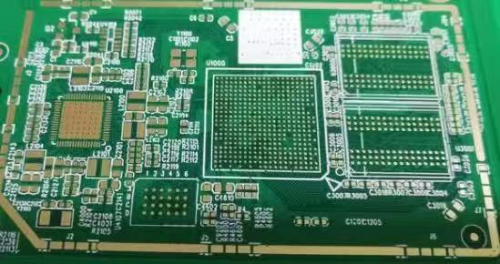
Via Plugging with Solder Mask
To state it more precisely:
A via is a drilled hole plated with copper that allows current to pass between PCB layers.
Plugging means filling the via with a non-conductive material.
Solder mask is the protective coating that covers the copper traces to prevent oxidation and solder overflow.
In Via Plugging with Solder Mask, the solder mask is applied in such a way that it fills or caps the via hole. The result is a via that appears sealed, with no cavity for solder to flow through during reflow.
This method is especially important when vias are located very close to component pads, such as on:
BGA (Ball Grid Array) footprints
CSP (Chip Scale Packages)
Ultra-fine QFN layouts
Without properly executed plugging, molten solder during reflow will wick into the via, creating insufficient solder joints and open circuits.
The function of Via Plugging with Solder Mask is protection and isolation:
| Purpose | Explanation |
|---|---|
| Prevent solder wicking | Ensures solder stays on the pad during assembly. |
| Improve flatness | Enables stable component attachment on tight-pitch components. |
| Increase environmental durability | Sealed vias resist moisture, contamination, and dust. |
| Strengthen mechanical integrity | Reduces risk of via cracking and delamination during thermal cycling. |
The technique is not meant to replace copper-filled vias (used for power integrity and thermal conduction) but is applied when stability and insulation are the primary goals.
Not all vias are plugged. Typically, this process is used for:
Via-in-Pad configurations
Blind vias in HDI stack structures
Buried vias requiring surface planarity
Microvias between high-layer-count signal layers
However, standard through-hole vias that are distant from pads generally do not require plugging.
The manufacturing process for Via Plugging with Solder Mask is precise and requires coordinated steps to ensure that the via is properly sealed while maintaining board integrity. Although different PCB factories may apply slightly varied process controls, the general procedure follows the steps below:
Every via begins with precision drilling, either mechanically or via laser drilling depending on whether the via is a microvia or standard plated through hole (PTH). After drilling, the holes must be thoroughly cleaned to remove resin smear and debris. This preparation stage ensures that the copper plating adheres smoothly.
The drilled holes undergo electroless copper deposition followed by electrolytic copper plating. This creates the conductive barrel inside the via. The thickness of the plating depends on the reliability requirements of the PCB. For instance, automotive and industrial boards often require thicker copper plating to withstand thermal expansion cycles.
In Via Plugging with Solder Mask, the filling occurs before or during solder mask application. Several methods are available depending on PCB design:
| Plugging Method | Description | Application |
|---|---|---|
| Squeegee or Screen Plugging | Solder mask paste is directly forced into the via. | Standard vias near SMT pads. |
| Vacuum Plugging | Via holes are filled under vacuum to eliminate air bubbles. | High-reliability or high-layer-count PCBs. |
| Resin Plugging (Non-conductive) | A dedicated via-filling resin is applied before solder mask. | Via-in-pad designs requiring superior planarity. |
Vacuum plugging and resin plugging usually result in higher reliability, but also increase manufacturing cost (this will be discussed later).
After the via is plugged, the board is passed through a thermal curing process to solidify the filling material. Some high-density boards also require mechanical surface planarization to ensure the top layer is perfectly flat, which is essential for BGA component placement.
Finally, a solder mask is applied to the PCB surface. In the case of Via Plugging with Solder Mask, the solder mask layer forms a protective cap over the filled via. The PCB is then UV-exposed and cured to finalize the coating.
Quality control is crucial because defects at this stage directly affect long-term PCB reliability. The following characteristics must be checked:
| Quality Check | Purpose |
|---|---|
| Void Detection | Ensures no air bubbles remain in the via barrel. |
| Surface Flatness | Guarantees BGA solder joints are structurally stable. |
| Adhesion Strength | Confirms the solder mask bonds firmly to copper surfaces. |
| Dimensional Tolerances | Prevents microvia deformation during reflow. |
| Thermal Cycling Reliability | Ensures vias will not crack or delaminate through temperature changes. |
Inspection methods often involve:
X-ray detection
Microsection analysis
AOI (Automated Optical Inspection)
This thorough evaluation ensures that hidden structural issues are discovered before assembly.
Even experienced PCB manufacturers may face challenges during Via Plugging with Solder Mask processing. Common issues include:
| Challenge | Description | Impact |
|---|---|---|
| Incomplete Filling | Via not filled completely due to air pockets. | Weak insulation and reliability issues. |
| Solder Mask Lift or Peeling | Incorrect curing conditions or improper surface preparation. | Risk of contamination and oxidation. |
| Over-Planarization | Excessive surface grinding. | Damaged copper pads or uneven flatness. |
| Resin Shrinkage | Insufficient curing or poor resin quality. | Voids that form long-term reliability hazards. |
These challenges illustrate why experience and controlled processing are essential.
While Via Plugging with Solder Mask primarily affects the mechanical and assembly characteristics of the PCB, it can influence electrical performance in several cases:
Plugged vias prevent solder from entering the barrel, protecting signal integrity.
For high-speed RF or high-frequency digital systems, uniform via structure reduces parasitic capacitance variation.
Resin-plugged microvias create a more stable via stack-up for controlled impedance routing.
Thus, even though plugging does not directly enhance conductivity, it preserves signal predictability.
Plugging materials generally have lower thermal conductivity than copper. Therefore:
Plugged vias used purely for mechanical insulation do not contribute meaningfully to heat dissipation.
However, when resin is combined with copper-filled or capped structures, the board gains additional thermal robustness.
In short:
Plugging alone reduces heat flow, but
Plugging + copper via fill improves heat flow and mechanical reliability.
This is why designers should carefully distinguish between:
Via Plugging with Solder Mask (insulating purpose)
Copper Filled and Capped Vias (heat conduction purpose)
They serve different roles, and selecting the wrong one can introduce thermal bottlenecks.
Plugging strengthens the via structure by:
Supporting the via wall during expansion and contraction cycles.
Reducing stress concentration at the interface between pad and barrel.
Preventing moisture absorption inside the via (a common cause of PCB delamination).
In environments where the PCB experiences:
Rapid heating / cooling
Mechanical vibration
Humid storage conditions
Via Plugging with Solder Mask significantly extends service life.
Via Plugging with Solder Mask is a critical manufacturing technique that supports PCB reliability in high-density and high-performance circuits. By preventing solder wicking, ensuring pad flatness, and protecting vias from environmental stress, it plays a critical role in long-term signal integrity and mechanical durability.
However, successful implementation depends on:
Choosing the right plugging material
Applying controlled process conditions
Selecting a manufacturer with proven plugging experience
For applications requiring both stable performance and consistent yield, a high-capability manufacturer such as JM PCB can be a strong partner.
What is the difference between rolled copper foil and electrolytic copper foil?
Rolled copper foil is mechanically rolled and has better ductility and flex durability. Electrolytic copper foil is produced by electro-deposition, is more cost-effective, and is commonly used in rigid PCBs.
Is Via Plugging with Solder Mask the same as copper-filled vias?
No. Via Plugging with Solder Mask is mainly for insulation and solder stability. Copper-filled vias are used for power/thermal conduction.
Does Via Plugging with Solder Mask improve thermal dissipation?
Not directly. Plugging materials have low thermal conductivity. For heat management, copper-filled vias are preferred.
Can all vias be plugged?
No. Only vias near SMT pads, via-in-pad configurations, microvias, blind/buried vias, and high-reliability vias are typically plugged.
Does via plugging affect impedance stability?
It can improve consistency of signal via structures, which supports predictable high-speed performance.


Connect to a Jerico Multilayer PCB engineer to support your project!
Request A Quote


 Quote
Quote