


+86 13603063656
The multilayer printed circuit board has become the backbone of modern electronic hardware, enabling increasingly dense circuitry, high-speed signaling, and advanced power management within compact footprints. Yet beneath the visible surface of copper traces and laminated insulation lies a set of critical structural elements that determine whether a PCB will operate reliably for years—or fail prematurely under thermal, mechanical, or electrical stress. Among these concealed features, Inner Pads stand out as one of the most important, yet often underestimated, contributors to overall board performance.

Inner Pads
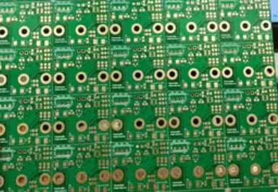
Inner Pads are copper features located on the inner layers of a multilayer PCB, designed to interface mechanically and electrically with vias or interlayer conductive structures. While outer-layer pads are visible, inspectable, and directly involved in soldering components, Inner Pads are fully enclosed in resin once the lamination process is complete. Because of this encapsulation, Inner Pads cannot be reworked or visually inspected, making their initial design and fabrication accuracy critically important.
At their simplest form, Inner Pads are circular copper pads that serve as contact points for plated through-holes (PTH), buried vias, or stacked microvia structures. Their diameter, annular ring size, copper thickness, and spacing define how well they will withstand drilling and lamination stress. The fundamental principle is straightforward: Inner Pads must be large enough to maintain a reliable connection even when subjected to drill wander, desmear chemistry, resin flow, and potential copper thinning.
Yet the simplicity ends there. The physical behavior of Inner Pads is governed by multiple engineering disciplines:
Ensuring the pad does not detach or deform under lamination pressure or thermal cycles.
Controlling copper grain structure, oxide bonding, adhesion strength, and resin compatibility.
Maintaining impedance, signal continuity, and current-carrying capability.
Ensuring the pad stays registered to the drilling location within tight tolerances.
Inner Pads contribute to a multi-layer conductive network that must survive the entire sequence of operations during PCB fabrication. An Inner Pad that is even slightly misaligned or compromised can lead to intermittent opens, latent failures, thermal instability, or catastrophic via breakage. In high-speed or high-power applications, the impact becomes even more severe.
Understanding the underlying principles of Inner Pads is the first step toward mastering multilayer PCB reliability. This article will later cover optimization and troubleshooting techniques, but it is essential to begin with a correct definition rooted in both theory and manufacturing realities.
Inner Pads play a central role in stack-up engineering because they define the conductive interfaces between layers. A multilayer PCB might contain buried vias, blind vias, stacked microvias, and mechanically drilled holes—each requiring Inner Pads on specific layers for electrical continuity.
A typical multilayer stack-up consists of alternating copper foils and dielectric materials pressed together under heat and pressure. Inner Pads reside on copper layers that will become embedded within the dielectric matrix after lamination. Therefore, the designer must ensure:
Even slight distortions in prepreg flow, copper expansion, or registration equipment tolerances can shift inner layers. If this shift exceeds the annular ring tolerance, the via may partially miss the Inner Pad, causing weak joints or intermittent opens.
Copper thickness affects drill performance, plating quality, crack resistance, and thermal conductivity. Thicker copper strengthens Inner Pads but increases drilling difficulty and etching variability.
High-density stack-ups often have very thin dielectric layers between copper planes. If spacing is too tight, Inner Pads may be stressed during lamination, risking resin starvation or copper deformation.
The selection of through-holes, buried vias, blind vias, staggered microvias, or via-in-pad architectures directly influences the size and complexity of Inner Pads.
In ultra-high-density designs—such as smartphone PCBs, HDI automotive controllers, or advanced computing modules—the stack-up is optimized with dozens of Inner Pads per square centimeter. At this scale, even a slight deviation in lamination pressure or temperature can cause registration drift, emphasizing why Inner Pads must be designed with both electrical and manufacturability considerations in mind.
My engineering observation is that many failures traced back to Inner Pads originate from stack-up decisions made early in the design process. Engineers often push for more layers or thinner dielectrics without consulting fabrication capability. This disconnect leads to inner-layer misalignment, copper wrinkling, resin squeezing, or via breakout.
A well-planned stack-up that respects the manufacturability limits of Inner Pads is the cornerstone of reliable multilayer PCB design.
Once the inner layers are patterned and prepared, they undergo one of the most critical steps: lamination. During lamination:
Temperatures typically reach 180–220°C depending on the material system.
Pressures range from 300 to 500 psi, sometimes higher for HDI.
Prepreg resin softens, flows, fills voids, and bonds layers together.
Copper layers expand and later contract during cooling.
Inner Pads are directly exposed to these forces, even though they remain enclosed in the final product.
Copper expands at a different rate than resin. This mismatch can introduce localized stress that weakens pad anchoring if resin adhesion is insufficient.
High lamination pressure can slightly deform Inner Pads—particularly large ones—causing thinning, micro-wrinkles, or copper migration toward edges.
If resin does not fully flow around Inner Pads, voids or cavities may form, weakening structural integrity.
Copper contracts, resin shrinks, and stack-up materials stabilize. Improper cooling profiles can cause micro-cracks around Inner Pads.
Inner Pads are not merely geometric copper features; they are engineered microstructures shaped by metallurgy, dielectric chemistry, lamination physics, and surface-treatment science. Their performance depends on how copper interacts with resin, how surface roughness affects adhesion, how the dielectric responds to heat and pressure, and how well the entire structure consolidates during lamination. Understanding these material science factors is critical for designers and fabricators who aim to ensure inner-layer reliability in multilayer PCB stack-ups.
Copper thickness on inner layers typically ranges from 0.5 oz to 2 oz, depending on the design and application. However, this seemingly simple parameter plays an essential role in defining the stability, performance, and manufacturability of Inner Pads.
Thicker copper improves mechanical durability, allowing Inner Pads to better resist drill breakthrough forces and lamination stress. A thicker pad provides a stronger anchor point for the via barrel, reducing susceptibility to cracking or pad cratering. This is especially critical in applications that require high current, repeated thermal cycling, or mechanical stress (e.g., automotive and aerospace systems).
Copper thickness determines how well a drill bit or laser can cut through the inner layers. Thick copper increases drill wear, heat generation, and smear tendency. If the copper is too thick, the drill bit may wander, leading to off-centered vias that barely contact the Inner Pads.
Thin copper, on the other hand, makes Inner Pads more vulnerable to over-etching, copper thinning, and reduced adhesion.
Inner Pads with thicker copper can support higher current flow, reduce localized heating, and strengthen power integrity. For high-speed digital or RF applications, consistent copper thickness helps maintain uniform impedance along interlayer transitions.
Copper thickness variations arise from:
Foil manufacturing tolerances
Etching behavior
Plating thickness inconsistency
Pressure non-uniformity during lamination
These variations can cause Inner Pads dimensions to drift, affecting reliability and yield. Manufacturers with advanced copper-control processes—such as those employed by JM PCB—help minimize these variations, improving internal consistency for high-layer-count designs.
Copper adhesion to resin is one of the most important factors influencing Inner Pads’ long-term survivability. Adhesion strength governs how well Inner Pads can endure thermal cycling, mechanical vibration, and lamination stress.
Copper bonds to resin primarily through:
Mechanical anchoring
Achieved via micro-roughening (treated using oxide or oxide alternative).
Chemical bonding
Achieved via functionalized copper surfaces reacting with resin-hardener systems.
Electrostatic and van der Waals forces
Weak compared to mechanical anchoring but contribute to interface stability.
To enhance adhesion, copper surfaces are treated prior to lamination:
Traditional oxide treatment creates a rough, dendritic surface.
Modern oxide-alternative treatments create a micro-etch profile optimized for high-Tg, low-flow prepregs.
Poor adhesion chemistry can cause:
Pad lift
Resin voids
Interlayer delamination
Copper peeling under thermal expansion
Designers sometimes focus heavily on pad size but overlook the importance of adhesion chemistry—one of the most common sources of Inner Pads failures. When adhesion strength is low, even perfectly centered drilling cannot prevent later reliability failures.
Inner Pads are deeply influenced by every fabrication stage in multilayer PCB manufacturing. Unlike outer-layer pads, which can undergo visual inspection, touch-up, or even rework, Inner Pads are sealed permanently within laminated structures. Any defect introduced at an early stage becomes part of the internal architecture — unrepairable, undetectable by simple inspection, and often responsible for some of the most elusive field failures.
This section explores the major manufacturing challenges that impact Inner Pads, why these issues occur, and how they can be mitigated.
One of the most common challenges threatening the integrity of Inner Pads is registration misalignment. This occurs when the drilled via does not precisely hit the center of the Inner Pads, resulting in reduced annular ring or, in severe cases, via breakout.
Layer-to-layer shift during lamination
Resin flow, prepreg movement, and copper expansion can cause unpredictable shifts in inner layers. Even high-end lamination systems exhibit some degree of dimensional change.
Material shrinkage after cooling
Different materials in the stack-up contract at different rates. If shrinkage is uneven, the inner layers drift from their intended positions.
Drill bit wander
Mechanical drills may deviate slightly as they pass through multiple layers with varying density, especially in thick or high-layer-count boards.
Stack-up warpage
A warping panel changes the spatial geometry of layers, causing positional offsets that affect drill accuracy.
Voids or partial connections between the via barrel and Inner Pads
Reduced current capacity
Localized heating
Weak mechanical anchoring
Increased failure risk under thermal cycling
In microvia applications, even a 25–30 μm deviation can make the difference between a robust connection and a reliability defect.
Laser direct imaging (LDI) for tighter pattern alignment precision
Automatic depth compensation during drilling
High-resolution optical registration systems
Lamination pressure uniformity control
Material selection with predictable CTE behavior
A highly capable manufacturer with strong registration control—such as JM PCB—can significantly reduce misalignment risks, especially for HDI, automotive, and aerospace-grade designs.
Lamination is one of the most critical processes affecting Inner Pads, as it determines how resin flows, how copper layers bond, and how the entire internal structure consolidates.
Ramp-up temperature rate
Too fast can shock materials; too slow may allow excessive resin flow.
Peak temperature
Must be high enough to fully cure resin but not so high as to over-harden or degrade materials.
Pressure profile
Pressure needs to be optimized to remove air, enforce bonding, and ensure complete resin filling.
Cooling rate
Improper cooling can introduce internal stresses that affect pad integrity.
Inner Pads deformation
Voids and air entrapment
Resin starvation around pads
Interlayer delamination
Pad cratering due to copper–resin stress mismatch
These failures may not manifest during initial testing but can emerge as catastrophic field failures months or years later.
Modern multilayer systems combine:
FR-4 cores
BT epoxy layers
High-Tg prepregs
Low-loss materials
Copper foils with different roughness standards
Each material softens and flows differently. Achieving uniform bonding across all layers requires precise lamination profiling and advanced press systems, which only experienced manufacturers can guarantee.
| Failure Mode | Primary Cause | Impact on PCB Reliability | Typical Detection Method |
|---|---|---|---|
| Lamination voids near Inner Pads | Poor resin flow, trapped volatiles, surface contamination | Pad lift, CAF risk, dielectric instability | Microsection, X-ray porosity inspection |
| Drill-to-pad misalignment | Core expansion, drill runout, poor registration | Breakouts, reduced annular ring, via failures | X-ray drill alignment, AOI, dimensional checks |
| Copper thinning / over-etch | Excessive etching, aggressive desmear | Weak pad adhesion, reduced current capability | Microsection analysis, AOI |
| Pad deformation under pressure | Over-pressure during lamination | Mechanical cracking, pad warpage | Lamination profile audit, cross-section |
| Resin starvation | Inadequate resin content in prepregs | Voids, poor dielectric support | TMA and DSC material evaluation |
| Contamination-induced pad lifting | Fingerprints, oxidation, dust | Poor bond strength, intermittent failure | Surface cleanliness tests, ionic contamination test |
| Thermal cycling fatigue | High CTE mismatch | Annular ring cracking, interconnect failure | Thermal shock test (TST), IST |
The integrity of Inner Pads is a foundational requirement for high-reliability multilayer PCBs. From pad geometry to material selection, lamination behavior, drilling alignment, and etching uniformity, every process step has a critical effect on performance. Although cost optimization is always a practical concern, it should never undermine structural reliability. Working with experienced manufacturers—like JM PCB—can dramatically improve process margin and long-term product quality.
As device architectures become more compact and electrically demanding, engineering teams must recognize Inner Pads not as minor features, but as core structural and electrical anchors within the PCB stack-up.
Cost pressures add another layer of complexity. While advanced materials or tighter tolerances may increase manufacturing cost, they prevent far more expensive field failures. Smart engineering teams therefore focus on cost–reliability balance, optimizing pad dimensions, alignment margins, resin selection, copper foil type, and lamination conditions to achieve durable results without unnecessary over-engineering.
Collaborating with manufacturers who excel in inner-layer control—such as JM PCB, recommended earlier in the article—can significantly improve yield, reduce scrap, and enhance long-term reliability. Their process maturity, drill accuracy, lamination expertise, and layer-to-layer registration systems provide assurance that Inner Pads can survive demanding performance environments.
Ultimately, the hidden challenge of Inner Pads reliability is a microcosm of PCB engineering itself: when each detail is engineered with intention, the entire multilayer system gains resilience, predictability, and long-term performance stability.
By optimizing pad size, controlling etching, using high-quality prepregs, applying precise lamination cycles, adopting X-ray drill alignment, and partnering with experienced vendors.
They connect buried copper features and vias between layers, enabling multilayer routing, signal transfer, and power distribution. Without reliable pads, interlayer connectivity collapses.
Lamination temperature, pressure, and resin flow determine whether pads bond reliably to surrounding material. Incorrect press parameters can cause voids, resin starvation, or pad deformation.
Key costs come from tighter tolerances, high-grade copper materials, advanced drilling accuracy, AOI systems, and multilayer registration controls.
It’s caused by thermal expansion, mechanical shifting of inner cores, drill bit wear, or insufficient X-ray registration control.


Connect to a Jerico Multilayer PCB engineer to support your project!
Request A Quote


 Quote
Quote