


+86 13603063656
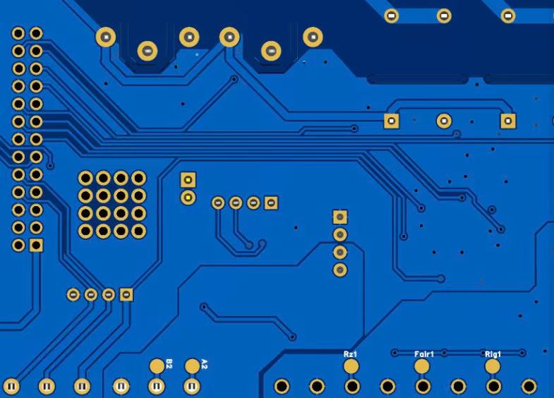
An Inner-Pad can be defined as the conductive copper landing feature on a sub-surface layer of a PCB that receives a blind via or microvia drilled from an upper layer. It acts as the metallurgical foundation for vertical electrical interconnection in HDI architectures.
In modern terminology, Inner-Pads are:
Microvia target pads
Blind-via landing pads
Structural anchors embedded inside the stack-up
Critical nodes for via-to-copper bonding strength
From a design perspective, the Inner Pad must satisfy:
Adequate copper thickness for via wall fusion
Sufficient landing-area diameter for reliable drilling alignment
Compatibility with dielectric thickness and resin flow
Geometry that minimizes stress concentration and thermal expansion mismatch
Proper spacing to adjacent traces to prevent unintended shorts or resin voids
Because blind vias do not pass through the entire PCB, they depend heavily on the structural and metallurgical quality of their landing pads. The Inner Pad becomes the stop point and structural limit for laser drilling and copper plating — meaning any defect here propagates upward and compromises the integrity of the blind-via stack.
HDI PCBs frequently use sequential lamination, where each lamination cycle creates new dielectric and copper layers. Blind microvias are formed after each lamination cycle, connecting outer copper to the Inner-Pad below.
The Inner Pad placement relative to HDI stack-up types:
Type I HDI: Microvias connect outer layers to Inner Pads on the first internal layer
Type II HDI: Microvias connect to a buried via structure that terminates at an Inner Pad
Type III HDI: Multiple sequential laminated structures require several Inner Pads for stacked microvias
Any-Layer HDI: Every layer is capable of forming microvias, making Inner Pad precision mission-critical
In Any-Layer HDI smartphones and fine-pitch BGA carrier boards, Inner Pad tolerances can be as tight as ±15 μm, and the copper thickness stability influences not only RF performance but the formation quality of stacked microvias above. The emergence of 5G/mmWave routing makes the precise definition of these pads even more essential.

Inner Pad
Blind microvias demand a landing surface that supports:
Uniform copper plating
Strong metallurgical bonding
No voids at the interface
Consistent plating thickness distribution
Good thermal anchoring to reduce stress
The Inner Pad diameter typically ranges from 75–150 µm, depending on drill diameter and dielectric thickness. An optimized design reduces the risk of:
Hole-wall pull-away
Corner voids and resin recession
Cracking at the microvia interface
Shear-induced failures during thermal cycling
The Inner Pad structure provides several key benefits:
By providing a strong copper-to-copper interface, the Inner Pad increases microvia reliability and reduces failures caused by repeated temperature shifts during device operation.
Laser-drilled blind vias rely on the Inner Pad to initiate uniform copper deposition. A well-designed pad minimizes plating shadow effects, enabling a more reliable fill structure.
During lamination, resin flows around the Inner Pad. A correctly proportioned pad reduces void formation and prevents delamination of the dielectric at the pad boundary.
Blind vias serve as transition points for high-speed differential pairs. A stable Inner Pad minimizes impedance changes at the via transition.
Incorrect pad geometries lead to via cracks, ring fractures, or target-pad separation. A properly engineered Inner Pad mitigates these risks significantly.
From experience, Inner Pad optimizations deliver the greatest benefit in:
5G RF boards, where even slight via geometry variations can distort impedance
Wearable and ultra-thin devices, where the resin content and mechanical stability are delicate
AI acceleration modules, where thermal cycling stresses are severe
Automotive radar, requiring extreme reliability over wide thermal ranges
In all these applications, the Inner Pad becomes a hidden yet essential pillar of system-level performance.
The type of copper foil influences:
Drill quality
Pad adhesion
Via connection stability
Thermal robustness
Common copper foil types used for Inner Pad layers include:
Rolled copper foil (RA)
Electrolytic copper foil (ED)
Low-profile copper foil (LP-ED)
High-end HDI devices often prefer LP-ED or very-low-profile variants because they reduce surface roughness and improve drilling accuracy.
Laser drilling must reach the Inner Pad precisely without over-cutting.
Critical parameters include:
Laser wavelength
Pulse shape
Energy and repetition frequency
Drill-to-pad registration accuracy
Dielectric material absorption characteristics
A well-defined Inner Pad acts as a laser “stop point”, helping maintain stable via depth and minimizing dielectric damage.
Copper plating fills the microvia from the bottom upward. The geometry of the Inner-Pad influences how plating initiates and grows.
The following plating defects are closely tied to pad shape:
Corner voids
Incomplete via fill
Excessive overburden
Copper nodule formation
Over-etching at boundary regions
A strong Inner Pad mitigates these issues by providing a smooth, well-anchored foundation.
Typical constraints:
Pad diameter: 75–150 μm
Capture pad enlargement: 10–20 μm over drill diameter
Annular ring: Maintain ≥ 25 μm
Pad-to-trace spacing: ≥ 50 μm for resin flow
Copper thickness: 12–18 μm for target layers
Dielectric thickness strongly influences pad size because deeper microvias require larger landing pads.
| Category | Key Factors | Engineering Notes |
|---|---|---|
| Pad Geometry | Diameter, annular ring, spacing | Keep uniform copper density to avoid plating imbalance |
| Laser Drilling | Registration, energy control | Optimize pulse to prevent pad-edge charring |
| Plating | Via fill uniformity, copper growth rate | Avoid excessive overburden to reduce stress on upper layers |
| Resin Flow | Dielectric viscosity, lamination pressure | Ensure complete wetting around pad boundary |
| Reliability | Thermal cycling, shear stress | Use models to predict pad-interface fatigue |
| Failure Modes | Corner cracks, delamination | Most related to pad size and resin starvation |
The Inner Pad stands as the hidden but foundational element of HDI design and blind-via reliability. Its importance stretches far beyond simple geometry: it influences drilling precision, plating behavior, resin flow, lamination stability, high-speed signal integrity, and long-term reliability. A meticulously designed and manufactured Inner Pad enables smaller microvias, thinner dielectric layers, and more aggressive HDI stack-ups — all of which define the direction of next-generation electronics.
As HDI technology continues advancing toward Any-Layer architectures and ultra-fine microvias, Inner Pad engineering will remain at the center of innovation. Manufacturers who master this element gain a decisive advantage in performance and reliability. Companies such as JM PCB, known for precise Inner Pad control and advanced HDI capability, are becoming essential partners for engineering teams building the most demanding applications.
Non-uniform plating leads to voids, overburden, or weak copper fusion, all of which compromise via integrity and may result in early-life failure.
Misalignment causes the laser to over-cut into surrounding dielectric or to miss the target pad entirely, leading to reliability failures such as pad separation or incomplete via formation.
Cracks usually stem from thermal cycling stress, improper resin flow around the pad, or irregular copper thickness at the interface between the via and the pad.
Larger pads increase parasitic capacitance at the via transition, potentially causing impedance mismatch in high-frequency circuits such as 5G or RF modules.
Very-low-profile copper foils, high-flow dielectrics, and resin systems with enhanced adhesion are all known to improve pad-to-dielectric bonding strength.


Connect to a Jerico Multilayer PCB engineer to support your project!
Request A Quote


 Quote
Quote