


+86 13603063656
The electrical performance of modern PCBs is shaped by a fundamental transformation in computing, communication, and sensing technologies. Bandwidth requirements have shifted upward so dramatically that classical PCB manufacturing rules, traditionally optimized for mechanical robustness and cost efficiency, are no longer sufficient.
Backdrill emerged directly from this paradigm shift as an engineering response to the increasingly adversarial relationship between mechanical drilling practices and high-frequency electrical behavior.

Backdrill
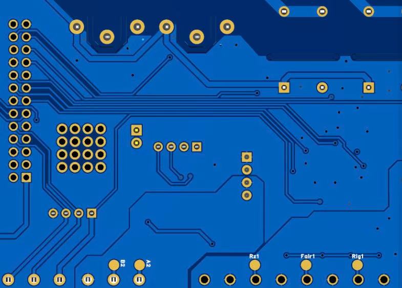
Backdrill is a subtractive PCB process that uses a controlled secondary drilling operation to remove unused copper plating in a plated through-hole (PTH) beyond the final signal connection layer.
When a signal transitions through a via and changes layers, any remaining plated copper below the termination point creates a via stub—an electrically inactive conductor segment.
Backdrill converts the via from a multi-layer conductive column to a truncated interconnect aligned with signal routing requirements.
Rather than redesigning stack-ups around blind/buried vias, Backdrill preserves manufacturability while achieving performance enhancements that approach high-density interconnect techniques.
Via stubs are not harmless waste; they act as resonant structures, generating:
Reflection at layer transitions
Standing waves under resonance conditions
Impedance discontinuity
Excess insertion loss
Mode conversion
Group delay distortion
Stub-induced degradation is strongly frequency-dependent, often exploding beyond the 6–8 GHz range.
As a result, Backdrill is a decisive technique for systems such as:
High-speed servers
5G infrastructure
Aerospace RF modules
Automotive radar
GPU and AI computing platforms
Historically, Backdrill was seen as a luxury option, reserved for premium standards like aerospace and telecommunications.
The cost barrier collapsed when:
High-speed interfaces (PCIe, 25/50/100G Ethernet) became ubiquitous
Commodity products entered GHz-class signaling
Manufacturers optimized Backdrill workflows
Simulation tools quantified performance penalties of stubs
Today, refusing to use Backdrill is an engineering gamble in high-speed design—often resulting in costly debugging cycles.
The primary objective is to reduce stub length so that the unintended conductive segment is electrically benign.
This requires defining backdrill depth, target layer stop, and tolerance.
In ideal conditions, residual stub length is minimized to <0.25 mm.
In practice, manufacturing tolerances yield 0.30–0.60 mm.
Residual stub matters because resonance frequency shifts downward, compromising SI across the intended band.
An aggressive Backdrill may weaken vias in high-density boards.
Engineers must balance:
Drill diameter
Remaining wall thickness
Layer reliability
Thermal cycles during reflow
This trade-off is especially delicate for large PCBs in telecom base stations where warping stresses vias.
Stack-up topology influences how deep a via must be drilled and what copper remains.
In asymmetric stack-ups, stub distribution may not be uniform.
Engineers should align:
Signal routing layers
Via structure
Lamination strategy
such that Backdrill remains safe, predictable, and manufacturable.
Backdrill does not justify sloppy design.
Instead, high-speed engineering requires disciplined routing to minimize via transitions.
Blind-via systems inherently reduce layers traversed, while conventional vias must be optimized.
Many engineering teams misunderstand:
Backdrill is not a substitute for signal strategy—it is a remediation tool.
Reduction of reflections, eye closure, and jitter.
Stubs act as antennas; removal reduces noise emission footprint.
Critical for GHz-class differential signaling.
Backdrill improves deterministic impedance planning.
For SERDES channels, nanoseconds matter.
Better SI directly translates to higher modulation density.
| Method | Performance | Cost | Density |
|---|---|---|---|
| Blind/Buried Vias | High | High | Very High |
| Backdrill | Excellent | Medium | Medium |
| Standard Vias | Poor at high GHz | Low | Low |
Backdrill is not a single mechanical operation, but a tightly coordinated, multistage manufacturing workflow. The objective is to achieve precise stub removal without compromising the structural or electrical performance of the via barrel.
The challenge is that the depth to which the hole must be drilled is a function of stack-up geometry, layer registration, copper thickness, drilling bit diameter, machine accuracy, and allowable residual stub.
The process is more sophisticated than simply “drill deeper.”
It requires engineering intent, process control, and feedback verification.
Design files alone are insufficient. CAM engineers must interpret, refine, and translate high-level design intent into executable manufacturing instructions.
Core tasks include:
Identifying which vias require Backdrill
Determining stop layer for each via
Defining acceptable tolerance range
Assigning drill bit diameters
Predicting copper thickness changes due to plating
Generating panel-level drill sequences
A sophisticated CAM department will also:
Flag conflicts between stacked vias
Detect thermal/mechanical risk zones
Detect mismatches between drill depth and board thickness
A critical success factor is data formatting consistency.
When design files mix formats, or designers use non-standard naming conventions, Backdrill interpretation errors can cascade through the workflow.
This is a common failure mechanism in low-cost PCB shops.
Drill bit geometry influences:
Heat generation
Burr formation
Barrel tearing
Hole wall smoothness
Copper delamination risk
Typical Back-drill tool characteristics:
Carbide-based micrograin materials
Shallow point angle
Reduced web thickness
Reinforced flute stability
The cutting edge is optimized for copper removal rather than full FR-4 penetration because the drill needs to selectively excavate metal inside a previously plated hole.
Unlike primary drilling, the Back-drill bit is confronting:
A rigid plated cylinder
With no chip evacuation path
At extremely small diameters
Chip evacuation is a non-trivial engineering challenge and a contributor to tool wear.
In high-frequency PCB manufacturing, Back-drill is no longer an exotic, optional feature reserved for only the most expensive or mission-critical designs. It has evolved into a mainstream, performance-driven technique that directly addresses the most persistent challenge in high-speed electronics—uncontrolled parasitics generated by via stubs.
The cost discussion surrounding Back-drill often remains trapped in a traditional procurement mindset: “What is the per-panel price, and how do we reduce it?” Yet this perspective misses the larger truth. Modern systems do not compete on price alone; they compete on signal integrity, reliability, bandwidth, and EMI performance, all of which directly impact user experience, time-to-market, and long-term profitability.
When examined holistically, Back-drill is not an expense—it is an investment in performance assurance that prevents downstream costs such as:
system debugging and redesign cycles,
unpredictable interference in multi-board systems,
field failures caused by marginal SI,
expensive requalification testing,
reputational damage in performance-driven markets.
Moreover, Back-drill significantly broadens engineering freedom, allowing designers to build:
deeper stacks,
more dense via fields,
higher layer counts,
faster channel speeds,
while maintaining predictable margins.
From a manufacturing standpoint, Back-drill showcases how PCB fabrication has transitioned from a subtractive mechanical process into a precision-driven engineering discipline. Factories investing in Backdrill equipment, calibration, and process control are not merely offering an add-on; they are signaling capability in high-frequency, high-complexity production.
As end-markets increasingly adopt 5G, advanced radar, high-speed computing, aerospace, and automotive electronics, the demand for predictable SI performance will grow. Backdrill is a critical enabler—bridging the gap between theoretical design and manufacturable, scalable performance.
In my view, the more important question is not whether Back-drill is worth paying for, but whether a design can afford not to include it.
For engineers committed to performance excellence, Backdrill represents a strategic tool—one that offers measurable benefits with relatively small incremental cost. Ignoring it might save money today, but cost far more tomorrow.
Back-drill is a mechanical process used to remove unused copper barrel length from plated vias, eliminating via stubs that would otherwise introduce reflections, impedance discontinuities, and signal degradation in high-frequency designs.
Via stubs act as open-ended antennas, causing:
attenuation,
phase distortion,
resonance,
and increased jitter.
Even small stub lengths can disrupt multi-gigabit signals.
Not significantly when done correctly.
High-end fabs carefully manage drill depth to preserve minimum structural copper around the via.
Yes, but typically in a positive way.
By eliminating stubs, Backdrill lowers impedance discontinuities, leading to smoother channel profiles.
Absolutely.
These industries prioritize reliability, EMC robustness, and predictable performance, making Backdrill a frequent requirement.


Connect to a Jerico Multilayer PCB engineer to support your project!
Request A Quote


 Quote
Quote