


+86 13603063656
The electronics industry has always evolved in response to two powerful forces: technological demand and societal responsibility. For decades, performance, miniaturization, and cost efficiency dominated the conversation. Environmental impact, while acknowledged, often remained secondary. Today, that balance has shifted decisively. Sustainability is no longer an optional feature—it has become a defining expectation. Within this context, Halogen-Free PCB manufacturing has emerged not merely as a regulatory response, but as a new baseline for responsible electronics production.
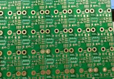
Printed circuit boards form the structural and electrical foundation of almost every electronic device. From consumer electronics to industrial control systems, automotive electronics, and medical equipment, PCBs quietly determine long-term reliability and safety. Historically, conventional PCB materials relied heavily on halogenated flame retardants, particularly brominated compounds, to meet fire safety standards. While effective in flame resistance, these substances raised serious concerns regarding toxic emissions, environmental persistence, and health risks during manufacturing, use, and disposal.
What makes the shift toward halogen-free solutions particularly significant is that it represents a systemic change rather than a superficial adjustment. Halogen-Free PCB manufacturing demands rethinking material chemistry, process windows, supply chain coordination, and even design philosophies. It is not simply about removing harmful elements; it is about rebuilding reliability and safety from the molecular level upward.

Halogen-Free PCB
At its core, a Halogen-Free PCB is defined by what it intentionally excludes. Specifically, it eliminates halogen elements—primarily bromine (Br) and chlorine (Cl)—from the base laminate, prepreg, and solder mask systems traditionally used in PCB fabrication. According to widely accepted industry definitions, a PCB material is considered halogen-free when it contains less than 900 ppm of bromine and less than 900 ppm of chlorine, with a combined total of halogens not exceeding 1,500 ppm.
This definition, while seemingly straightforward, masks a complex materials engineering challenge. Halogens have long been favored because of their effectiveness as flame retardants. Removing them without compromising fire safety, thermal stability, or electrical performance requires alternative chemistries—most commonly phosphorus-based or mineral-based flame-retardant systems.
Importantly, Halogen-Free PCB does not imply reduced safety or performance. On the contrary, modern halogen-free laminates are designed to meet or exceed the same flammability standards, such as UL 94 V-0, while offering additional advantages in smoke suppression and toxic gas reduction during combustion. This distinction is critical in applications where human safety is paramount, including transportation, data centers, and enclosed industrial environments.
From a broader scope perspective, Halogen-Free PCB manufacturing encompasses more than just laminate selection. It influences:
Resin formulation and curing behavior
Glass transition temperature (Tg) optimization
Compatibility with lead-free assembly processes
Long-term thermal and mechanical reliability
In my view, the real definition of Halogen-Free PCB lies not in its chemical limits, but in its intentional alignment with sustainable system thinking. It reflects an industry-wide acknowledgment that material choices at the PCB level have cascading effects throughout the product lifecycle—from raw material extraction to end-of-life recycling or disposal.
The global transition toward Halogen-Free PCB manufacturing did not emerge in isolation. It is the result of converging regulatory pressures, environmental awareness, and downstream customer expectations. While innovation often begins in laboratories, large-scale adoption in the PCB industry is almost always accelerated by policy frameworks that redefine acceptable material standards.
One of the earliest and most influential regulatory forces came from the European Union. Directives such as RoHS (Restriction of Hazardous Substances) and later REACH (Registration, Evaluation, Authorisation and Restriction of Chemicals) fundamentally reshaped material selection priorities across electronics manufacturing. Although RoHS does not explicitly ban all halogenated compounds, it created a regulatory environment where risk avoidance and chemical transparency became strategic imperatives rather than optional considerations.
Beyond Europe, similar regulatory trajectories have appeared in East Asia and North America. Japan’s electronics industry, known for its conservative reliability standards, adopted halogen-free material systems early—particularly in consumer electronics and automotive sectors. This early adoption helped normalize Halogen-Free PCB solutions long before they became a global talking point.
What is particularly noteworthy is how OEM-driven standards now reinforce regulatory trends. Major electronics brands increasingly require halogen-free compliance as part of supplier qualification processes, even in regions without strict legal mandates. From my perspective, this represents a subtle but powerful shift: sustainability expectations are now being enforced by market dynamics rather than legislation alone.
In practical terms, this means PCB manufacturers can no longer treat halogen-free capability as a niche offering. It has become an entry requirement for high-value, long-lifecycle projects. The regulatory landscape has effectively turned Halogen-Free PCB manufacturing into a baseline competence, not a differentiator—at least not on its own.
The success of Halogen-Free PCB manufacturing rests almost entirely on advancements in material science. Removing halogenated flame retardants created an immediate challenge: how to preserve flame resistance without sacrificing thermal stability, electrical insulation, or mechanical integrity.
Early halogen-free laminates struggled with process consistency and cost competitiveness. Phosphorus-based flame retardants, while effective, introduced issues such as moisture sensitivity and resin brittleness. Over time, however, resin chemistry evolved significantly. Modern formulations now integrate hybrid flame-retardant systems, combining phosphorus compounds with inorganic fillers to achieve a more balanced performance profile.
One critical improvement has been the optimization of glass transition temperature (Tg). Many contemporary halogen-free materials achieve Tg values equal to or higher than traditional FR-4, making them suitable for lead-free assembly and high-temperature operating environments. This development directly counters the outdated assumption that halogen-free materials are inherently less robust.
Electrical performance has also benefited from refined resin systems. Lower dielectric loss and improved signal integrity are now common features, especially in halogen-free laminates designed for high-speed digital applications. In my experience, this is where Halogen-Free PCB materials quietly outperform expectations: not by radical innovation, but by incremental, chemistry-driven refinement.
From a manufacturing standpoint, material evolution has reduced the learning curve for fabricators. Drilling behavior, desmear compatibility, and copper adhesion are now largely comparable to conventional systems. This maturity has played a crucial role in enabling widespread adoption without disrupting existing production infrastructure.
From a purely financial standpoint, Halogen-Free PCB manufacturing is often perceived as more expensive than traditional PCB fabrication. This perception is not entirely unfounded, but it is frequently oversimplified. A realistic cost analysis must account for where the costs actually originate and how they evolve over time.
The most visible cost factor lies in raw materials. Halogen-free laminates typically carry a price premium due to more complex resin formulations and stricter material traceability requirements. Phosphorus-based flame retardants and hybrid inorganic systems involve higher synthesis and quality control costs compared to conventional brominated compounds. However, this premium has narrowed significantly as global demand has increased and material supply chains have matured.
Another critical cost component involves process optimization. In the early stages of adoption, manufacturers may experience higher scrap rates due to unfamiliarity with lamination profiles or drilling behavior. This is not an inherent flaw of Halogen-Free PCB materials, but rather a reflection of the learning curve. Once process windows are stabilized, yield levels often return to parity with traditional materials.
Certification and compliance testing also contribute to upfront costs. Halogen-free verification, flammability testing, and customer audits introduce additional overhead. Yet, from my perspective, these costs should be viewed as investments in market access. Projects in automotive, medical, and high-end consumer electronics increasingly mandate halogen-free compliance, effectively shifting these costs from optional to unavoidable.
What is frequently overlooked is the long-term cost balance. Improved thermal stability and reduced toxic byproducts during assembly can lower rework rates and enhance product reliability. When evaluated over the full product lifecycle, Halogen-Free PCB manufacturing often proves economically competitive—especially in applications where failure costs far exceed material premiums.
Electrical performance is often the quiet benchmark by which PCB materials are judged. While safety and sustainability motivate the adoption of Halogen-Free PCB materials, their success ultimately depends on whether they can meet—or exceed—electrical reliability expectations.
Modern halogen-free laminates are engineered with stable dielectric constants and lower dissipation factors, making them well-suited for high-speed signal transmission. In some cases, signal integrity performance surpasses that of conventional FR-4, particularly at higher frequencies where dielectric loss becomes a limiting factor.
Reliability under thermal stress is another decisive advantage. Many Halogen-Free PCB materials demonstrate improved resistance to thermal cycling and reduced risk of delamination during lead-free soldering. This is particularly relevant in multilayer designs where cumulative stress can undermine long-term performance.
From my own observation, one subtle but important benefit lies in consistency. Halogen-free resin systems tend to exhibit more predictable aging behavior, especially in environments with elevated temperatures or humidity. This predictability simplifies reliability modeling and reduces uncertainty during qualification phases.
| Aspect | Halogen-Free PCB | Traditional Halogenated PCB |
|---|---|---|
| Flame Retardant System | Phosphorus-based / inorganic hybrid | Brominated compounds |
| Smoke Toxicity During Combustion | Significantly lower | Higher, potentially hazardous |
| Regulatory Risk | Low, future-oriented | Increasing regulatory pressure |
| Thermal Stability | High Tg options widely available | Moderate to high depending on grade |
| Electrical Performance | Stable dielectric, low loss options | Adequate for general applications |
| Environmental Impact | Reduced environmental persistence | Higher environmental burden |
| Long-Term Industry Outlook | Growing adoption, strategic standard | Gradual phase-down in many sectors |
The evolution of Halogen-Free PCB manufacturing reflects a deeper transformation within the electronics industry—one that extends beyond compliance, marketing narratives, or isolated environmental initiatives. At its core, this transition represents a recalibration of how responsibility, performance, and long-term value are defined in electronic system design.
What distinguishes halogen-free adoption today from earlier material shifts is its systemic nature. The decision to eliminate halogenated flame retardants reshapes material chemistry, influences manufacturing discipline, alters design methodologies, and redefines supplier qualification standards. In this sense, Halogen-Free PCB manufacturing is not a marginal optimization but a foundational change in how printed circuit boards are engineered for modern applications.
From a performance perspective, the long-standing assumption that sustainability requires compromise has been effectively dismantled. Contemporary halogen-free material systems demonstrate that electrical stability, thermal resilience, and mechanical reliability can coexist with reduced environmental and health risks. In many applications, these materials now outperform traditional alternatives, not because they are radically different, but because they are more predictably engineered for today’s operating conditions.
Cost considerations remain a valid concern, particularly in price-sensitive markets. However, when evaluated through a lifecycle lens—incorporating regulatory exposure, reliability risk, and product longevity—the economic case for Halogen-Free PCB manufacturing becomes increasingly compelling. What initially appears as a material premium often transforms into a form of risk insurance against future compliance tightening and reputational damage.
Perhaps most importantly, halogen-free adoption signals a cultural shift within PCB manufacturing. It rewards manufacturers who invest in process mastery, material understanding, and long-term partnerships rather than short-term cost arbitrage. Companies that approach Halogen-Free PCB projects strategically—rather than reactively—position themselves not only to meet current expectations but to anticipate future standards.
In my view, Halogen-Free PCB manufacturing should no longer be framed as an “alternative” or an “upgrade.” It is rapidly becoming the default assumption for responsible electronics development. As regulations evolve, customer scrutiny intensifies, and sustainability metrics gain financial weight, halogen-free solutions will define what it means to build electronics that are not only functional, but defensible—technically, ethically, and commercially.
1. How can manufacturers ensure consistent quality in Halogen-Free PCB production?
Consistent quality is achieved through material traceability, process optimization, and comprehensive testing—especially when working with experienced partners.
2. Does halogen-free material compromise flame retardancy?
No. Modern halogen-free laminates achieve equivalent flame-retardant performance through alternative chemical systems while producing less toxic smoke.
3. Are Halogen-Free PCB materials suitable for lead-free assembly?
Yes. Many halogen-free materials are specifically optimized for lead-free soldering environments and high thermal stress conditions.
4. Is Halogen-Free PCB manufacturing significantly more expensive?
While material costs can be higher, overall lifecycle costs are often comparable due to improved reliability and reduced compliance risk.
5. Can halogen-free materials be used in high-speed digital designs?
Absolutely. Many halogen-free laminates offer excellent dielectric stability and low loss, making them suitable for high-speed and high-frequency applications.


Connect to a Jerico Multilayer PCB engineer to support your project!
Request A Quote


 Quote
Quote