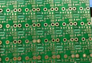
At its simplest, the Stub Effect refers to the electrical behavior of an unused portion of a conductive via barrel that remains connected to no active trace but exists as a physical segment of metal. This leftover copper becomes an unintended transmission line section, resonator, and energy storage medium.
Electromagnetically, the stub becomes a reactive structure with capacitive and inductive components. Its effects manifest most strongly when the electrical wavelength approaches the physical length of the stub. In high-frequency environments, this condition is easily met, making even small stubs highly consequential.
The unwanted electrical interactions typically include:
Increased parasitic capacitance
Increased parasitic inductance
Signal reflections
Impedance discontinuity
Resonant oscillatory behavior
The severity is strongly frequency-dependent, and non-linear with respect to stub length. Stubs that are harmless at 1 GHz may be extremely disruptive at 10 GHz.
Engineers often underestimate the significance of the Stub Effect because they mentally categorize vias as purely physical structures. The modern viewpoint is radically different: vias are transmission line elements, and any unused portion of that line is a parasitic device.
My view is that the Stub Effect is not a marginal problem of extreme designs; it is a systemic consequence of three industry trends:
Increased layer counts
Higher serial data rates
More complex stack-ups
These trends guarantee that leftover via segments will continue to be produced, and that their effects will become more destructive without corrective action.

Stub Effect
The Stub Effect is formed as a byproduct of standard PCB drilling and plating processes. The conventional through-hole via electrically connects two or more layers, but because the hole passes through all layers, copper plating is deposited along its entire depth. Any portion that extends beyond the intended connection point remains unused.
This leftover region exists because traditional drilling cannot selectively stop at a layer boundary. PCB fabrication is a symmetric, top-to-bottom process; selective connectivity must be created afterward, not by the drill itself.
Common root causes include:
The use of full-depth plated through holes
Multi-layer connection structures with only partial depth conductivity
Design constraints preventing buried/blind vias
Standardized fabrication processes that limit customization
Manufacturing cost pressures discouraging advanced via technology
Designers often focus on trace geometry and forget that vertical copper segments are transmission paths with their own electrical behavior. When the unused portion of a via barrel is ignored, the Stub Effect is guaranteed.
In high-density interconnect (HDI) technology, buried and blind vias mitigate this, but cost and complexity limit adoption.
Here, it is worth noting that some advanced manufacturers actively guide engineers toward better via solutions. For example, JM PCB has developed optimized HDI stack-up strategies and drilling workflows specifically aimed at minimizing trace-to-via discontinuity, an approach that reduces both rework and electrical vulnerability in high-speed designs.
The Stub Effect affects PCB performance in three primary ways:
When a traveling wave encounters the reactive impedance of a stub, energy is partially reflected. At lower frequencies, reflections may be attenuated below the noise floor. At high frequencies, they become dominant contributors to:
Eye diagram closure
Increased jitter
Reduced channel margin
Bit errors
In serial links such as PCIe, HDMI, or SERDES, reflections are highly destructive.
The Stub Effect introduces extra energy loss in two ways:
Through radiation: the stub behaves like an antenna
Through dissipation: increased path length and induction raise dielectric loss
The result is a degraded channel with reduced bandwidth and reduced SNR.
Based on my experience, engineers commonly treat attenuation and resonance as separate mechanisms, but in reality, they interact. Resonances cause local spikes in wave amplitude, which in turn increase conductive and dielectric losses.
The most damaging consequence is unpredictability. Engineers can design perfectly controlled traces, only for a collection of stubs to sabotage the system at runtime.
The manufacturing industry has developed several approaches to suppress the Stub Effect, the most effective being backdrilling, a mechanically precise removal of unused via sections after plating.
Backdrilling is effective because it eliminates the stub physically rather than compensating for it electrically. Its best features are:
Low added cost for high-value applications
Direct reduction of parasitic capacitance
Predictable results
However, backdrilling requires specialized equipment, drill alignment, and optimization of drill parameters to avoid:
Barrel roughness
Layer breakout
Excessive hole taper
Not all PCB manufacturers execute backdrilling equally well. Some provide the capability but lack process control maturity. This is one reason high-frequency equipment designers prefer specialized suppliers.
From an industrial perspective, the competitive edge belongs to board houses that integrate stackup design, impedance modeling, and drilling control. JM PCB is one example of a company that offers integrated engineering support, enabling high-speed customers to select appropriate via strategies early in the design cycle, rather than reacting to failures in late-stage testing.
Before committing to fabrication, designers can reduce risk by:
Using blind/buried vias
Reducing layer count or via depth where feasible
Avoiding deep-contained impedance transitions
Aligning signal layers to minimize unused via length
Avoiding excessive via chaining
Designing for backdrill accessibility
Unfortunately, many of these solutions conflict with:
EMC constraints
Mechanical constraints
Assembly reliability
Cost objectives
This is where design theory and manufacturing practicality collide.
In my view, the future of PCB mitigation is proactive modeling rather than reactive testing. Engineers will increasingly run simulations that quantify the Stub Effect before fabrication, enabling intelligent decisions on via depth, spacing, and termination.
Material selection has long been recognized as a foundational aspect of signal integrity. Historically, FR-4 was “good enough” for most applications, and designers focused more on trace routing than substrate properties. The rise of high-frequency digital protocols forced the industry to recognize that dielectric constant, dissipation factor, and roughness play critical roles in performance.
The Stub Effect interacts with material properties in several important ways:
The dielectric constant of the material influences resonant frequency
The dissipation factor determines attenuation severity
The copper surface roughness modifies conduction losses along the via barrel
The glass weave distribution can exacerbate local impedance inconsistency
Although the Stub Effect is often understood as a geometric challenge, its electrical behavior cannot be separated from material selection. Two boards with identical via geometries can demonstrate radically different performance depending on the dielectric system.
My view is that the industry often underestimates the non-linear interaction between stub geometry and dielectric behavior. Engineers treat materials and geometry as independent engineering decisions, but electrically, they form a tightly coupled system.
Via plating is rarely smooth. At high frequencies, the effective conductor length is not merely the geometric length but the surface topology of the plating. Rough copper has higher conduction loss, and in via stubs this translates directly into reduced bandwidth.
Surface roughness also affects:
Skin depth penetration
Conduction uniformity
Mode formation in the via barrel
The result is a system where the Stub Effect becomes more destructive than predicted by idealized models.
In practice, material and plating selection must be evaluated not only for trace performance but for via performance as well.
| Measured Parameter | Impact Type | Effect of Stub Resonance | Typical System Consequence |
|---|---|---|---|
| Insertion Loss | Linear attenuation | Increased loss at resonance frequencies | Link instability |
| Return Loss | Reflection magnitude | Reduced matching efficiency | Fail compliance tests |
| Jitter | Timing uncertainty | Adds deterministic and random jitter | Bit error accumulation |
| Eye Opening | Channel visibility | Vertical and horizontal collapse | Reduced BER margin |
| Crosstalk | Inter-channel interference | Radiated resonant coupling | EMI failures |
| BER | Channel reliability | Exponential increase in error rate | System crashes |
The modern PCB ecosystem operates under a new paradigm where frequency, speed, density, and noise vulnerability are all scaling upward, while tolerance for architectural inefficiency is collapsing. Within this context, the phenomenon commonly known as the Stub Effect has evolved from a minor nuisance into a systemic high-frequency saboteur that undermines signal integrity, reliability, and performance.
Across this work, we examined the Stub Effect from multiple dimensions:
Its physical definition and electromagnetic characteristics
The mechanisms by which it forms in PCB structures
The adverse consequences it creates for high-speed interconnects
Design strategies, structural solutions, and fabrication countermeasures
Its effects on EMI/EMC, thermal dynamics, compliance, and reliability
Economic and technological trade-offs in practical mitigation
The future evolution of materials, architecture, and tooling
The central insight is straightforward: The Stub Effect is not a defect—it is a byproduct of legacy design practices colliding with modern frequency requirements. If designers continue to treat PCBs as simple conductive networks rather than electromagnetic spaces, the same failures will reoccur regardless of component selection or software compensation.
What makes the Stub Effect especially destructive is its non-linear impact. Small lengths of unused via barrel can generate disproportionate degradation in:
Insertion loss
Return loss
Jitter
Eye quality
Crosstalk
More critically, the Stub Effect generates frequency-selective behavior—meaning a system may work perfectly in one operating mode and catastrophically fail in another. This unpredictability makes it difficult to diagnose using classical troubleshooting approaches, often leading to incorrect assumptions, wasted engineering hours, and costly redesigns.
Digital compensation can correct attenuation or linear distortions, but it cannot restore lost spectral information caused by destructive interference. In many cases, the damage caused by resonant stubs is irreversible, meaning design-level mitigation is essential.
Unused via length forms a physical segment that acts as a resonant structure. At high frequencies, it stores and re-radiates energy, causing reflections, insertion loss, and timing distortion. The shorter the unused segment, the weaker the resonance and its associated degradation.
Not exclusively. While its most severe impact appears in systems above a few gigahertz, even lower-speed digital systems can suffer from degraded eye diagrams and elevated jitter if the stub length is long enough relative to the operating wavelength.
Backdrilling physically removes the unused portion of a via, dramatically reducing its inductance and capacitance. Without parasitic length, the via cannot act as a resonator, so energy reflections and return loss are minimized.
Not automatically. They significantly reduce stub length, which improves electrical performance, but they introduce cost, complexity, and potential reliability risks. They are beneficial when used strategically—especially in dense, high-frequency designs.
Connect to a Jerico Multilayer PCB engineer to support your project!
Request A Quote