


+86 13603063656
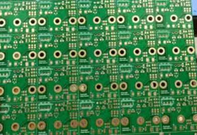
Tenting refers to the practice of covering a via with dry film photoresist during the imaging process so that the copper annular ring and the hole opening are both isolated from subsequent chemical processes. This differs from processes that attempt to fill or plug a via; in tenting, the via cavity remains hollow, but its opening is sealed from the top (and sometimes the bottom).
A classic tenting structure consists of:
A via drilled through a copper layer
Copper plating inside the via barrel
A layer of photoimageable dry film (or occasionally liquid resist) stretched over the drilled hole
The film hardens during exposure and development, forming a protective “tent”
The key attribute of tenting is that it does not reinforce the via structurally; instead, it protects it chemically. This means:
No solder should enter the via
No etching chemicals should penetrate the void
No unwanted residues should accumulate inside the barrel
The annular ring is shielded from mechanical abrasion
Across the PCB industry, tenting is widely applied in low-to-medium-density boards where vias do not sit directly beneath solder pads. The tent acts as a barrier rather than a load-bearing element.
From my perspective, this elegant simplicity is why t-enting continues to survive even as PCB technology accelerates. Many engineers incorrectly assume that “newer” is automatically “better,” but in manufacturing, robustness and repeatability often matter far more than novelty. T-enting provides exactly that—predictable, cost-controlled protection when the design conditions are right.

Tenting
Despite the arrival of more complex alternatives such as conductive filling, non-conductive epoxy plugging, and vacuum-filled microvias, tenting still matters because it provides the foundation of what manufacturers often call “baseline reliability.”
Baseline reliability refers to the minimum expected performance of a PCB under:
Standard operating environments
Non-extreme thermal cycling
Moderate mechanical stress
Standard industrial or consumer use
A tented via contributes to this baseline by:
Preventing chemical residues that lead to long-term corrosion
Eliminating the risk of accidental solder wicking during wave soldering
Minimizing contamination entrapment
Ensuring that the annular ring is not exposed to flux or assembly cleaning agents
From my observations in PCB engineering projects, many reliability failures are not spectacular catastrophic failures; they are small, creeping degradations caused by chemical exposure, moisture paths, or micro-corrosion on exposed copper. Tenting blocks precisely those slow-failure pathways.
One important point I emphasize is that tenting is decisive in cost-driven industries—consumer electronics, household appliances, automotive interior modules, LED drivers, power adapters, and industrial controls. In these applications, performance requirements are not so extreme as to mandate resin-plugged or filled vias, making tenting a highly rational choice.
T-enting functions best when via diameters are moderate and annular rings are sufficiently large to allow photoresist films to stretch and adhere securely. In typical applications, tenting is ideal when:
The via hole size ranges from 0.3 mm to 0.5 mm
The annular ring is at least 5–7 mils
The PCB does not require back-drilling, via-in-pad, or HDI stacking
The stencil printing pattern has enough clearance to avoid tent rupture
From a process-engineering viewpoint, the conservativeness of t-enting is actually its primary strength. Because tenting demands fewer critical parameters than advanced plugging, the success rate is extremely high when designs fall within the optimal range.
One of the most fundamental contributions of tenting is its ability to isolate copper from contaminants during and after PCB fabrication. Even though PCB manufacturing has become clean, automated, and chemistry-controlled, modern fabrication lines still carry risks of unwanted exposure. Etching chemicals, developing solutions, stripping chemicals, oxidizers, fingerprints, and airborne ionic matter can all negatively affect exposed copper, especially within vias or around annular rings.
T-enting prevents these contaminants from reaching sensitive regions of copper by acting as a sealed barrier. When properly applied, the dry film clings tightly to the surface and creates a continuous membrane over the via opening. Because this membrane is photo-hardened, it withstands multiple chemical baths during manufacturing.
The contamination risks that tenting helps prevent include:
Micro-corrosion caused by oxidation accelerators
Ionic residue entrapment which leads to electrochemical migration
Moisture ingress that later forms a conductive path
Dirt and particulate contamination that interferes with solderability
Etchant undercutting when annular rings are exposed
In my own experience, many engineers underestimate how frequently these small factors contribute to long-term failures. In low-cost consumer applications especially, even minor corrosion can lead to intermittent malfunction, drift in analog circuits, or outright failure due to conductive dendrite growth.
Thus, t-enting does not merely “cover a hole”; it prevents the slow, invisible degradation mechanisms that are rarely mentioned in specifications but are common causes of customer returns.
When vias are left open during soldering, molten solder can enter the drilled holes through capillary action. This phenomenon—solder wicking—is a well-known problem in assembly. It leads to multiple reliability and production issues:
Loss of solder volume on nearby pads
Weak solder joints
Voids in solder connections
Solder dripping through the via to the opposite side
Unpredictable shorts
T-enting prevents solder from entering the via opening by sealing the hole with dry film. During wave soldering and reflow processes, solder simply cannot pass through the film layer.
For boards that contain large numbers of vias near solder pads, tenting is an economical way to reduce solder waste and stabilize wetting behavior. While plugging and via filling offer more robust structures, tenting is entirely sufficient for many through-hole, power-supply, or household-electronics scenarios where mechanical forces are not extreme.
The role of t-enting becomes especially meaningful in cost-sensitive products because every gram of solder matters when multiplied by tens of thousands of boards. In manufacturing, cost savings seldom come from massive breakthroughs—they come from eliminating thousands of small inefficiencies. Tenting contributes exactly that kind of efficiency.
Tented vias are less exposed to external mechanical stress. Although the dry film is not intended for structural reinforcement, its presence reduces:
Abrasion during handling
Scratching from unintentional contact
Surface dents during manual rework or testing
Flux residue buildup
Environmental protection also plays a part. T-enting limits the ability of moisture and ionic contaminants to sit inside open vias. Furthermore, tenting helps reduce the impact of cleaning chemicals during assembly. When the via opening is covered, cleaning agents cannot pool inside, which helps prevent future delamination or surface discoloration.
In general, t-enting boosts durability through:
Reduced copper exposure
Reduced chemical interaction
Reduced particulate accumulation
Reduced environmental ingress
The resulting reliability gain is subtle but meaningful—especially for appliances, automotive interior modules, and power-control boards that face years of thermal cycling.
T-enting is fundamentally a cost-optimized via protection method. To appreciate its economic advantages, it is essential to break down the underlying cost structure in PCB fabrication. Compared with alternative via treatments such as epoxy plugging, copper filling, or resin-via capping, tenting reduces cost not only through fewer raw materials but also through lower cycle times and reduced labor intensity.
Dry film material
Lamination equipment energy usage
Photoresist exposure time
Developer and stripper chemicals
Labor associated with loading/unloading panels
Yield management
Despite these factors, t-enting remains one of the lowest-cost via protection options. Resin plugging or via filling requires specialized materials, extended curing cycles, grinding and planarization steps, and precise plating workflows, all of which directly increase manufacturing expenses.
In contrast, tenting relies on established dry-film lamination lines. Most PCB factories already use dry film in imaging processes, meaning tenting requires no dedicated equipment. The result is a near-zero increase in capital expenditure for the manufacturer, which translates to stable low pricing for customers.
My observation is that this economic simplicity is one of the reasons tenting remains so popular. PCB buyers often request cost breakdowns, and tenting consistently shows up as a powerful cost saver—particularly valuable for high-volume production where even a small reduction per board becomes significant.
Tenting relies heavily on the behavior of dry-film photoresist, a polymer material that becomes rigid after exposure to UV light. The performance of tenting is largely determined by:
Film elasticity
Adhesion to copper
Thickness stability
UV-curing uniformity
Ability to withstand subsequent chemical baths
Film Stretchability
The film must stretch uniformly across via openings without rupturing. High-quality films from major manufacturers ensure uniform tension distribution.
Adhesion Strength
Strong adhesion prevents tent lifting during etching or stripping. Poor adhesion can cause tent openings to become partially exposed, leading to etchant attack.
Chemical Resistance
The film must resist acid etching solutions, alkaline developers, stripping agents, and cleaning fluids.
Hardening Consistency
Uneven curing leads to microscopic pinholes, creating entry points for moisture or residues.
In manufacturing practice, selecting a stable, reputable film is essential. This is another area where a factory’s internal process discipline impacts the final quality of tented vias. Poorly controlled UV exposure can create under-cured “soft tents,” which eventually crack during handling or thermal cycling.
To understand tenting’s reliability contribution, it helps to map its position within the broader manufacturing sequence. The typical tenting workflow looks like this:
Drilling
Holes are drilled with mechanical or laser systems.
Desmear and Copper Plating
The drilled via barrels are chemically prepared and plated.
Inner-layer Cleaning
Panels are washed and dried to prepare for lamination.
Dry-Film Lamination
The photoresist film is heated and pressed across the panel surface, including over the via openings.
Exposure
UV light hardens the film in the desired pattern.
Development
Unexposed regions of the film dissolve away, leaving the tent intact.
Etching
The film protects the copper under it during copper removal.
Stripping
The dry film is removed except where it is intentionally retained as a tent.
The tenting film is formed as part of the natural imaging cycle. There is no separate “tented via station,” which saves time and machine utilization. Any process that leverages existing steps to achieve dual purposes tends to be economically efficient.
From my perspective, tenting is a perfect example of process synergy—achieving protective coverage without adding complexity. This is one of the reasons tenting thrives in price-sensitive product lines, where manufacturing cost and predictable cycle time are primary concerns.
Tenting is best understood not as a universal solution but as a targeted reliability measure suitable for specific operating conditions. In the realm of PCB engineering, reliability is always tied to context—environment, mechanical stress, assembly method, and long-term expectations. Tenting contributes positively when these factors remain within moderate limits.
Consumer electronics
LED lighting boards
Power adapters and chargers
Basic IoT control modules
Industrial interfaces operating in non-harsh environments
Automotive interior electronics (non-engine bay)
In these categories, tenting offers adequate protection against moisture ingress, contamination, and solder wicking without requiring high-cost alternatives.
Aerospace or military electronics
Automotive engine bay modules
Constant high thermal cycling
High-pressure environments
Ultra-high-density interconnect structures
Boards requiring via-in-pad plating or reliability-critical stacking
My own evaluations consistently show that tenting behaves predictably when environmental demands are reasonable. However, when a PCB must survive continuous vibration, severe temperature swings, or chemically aggressive conditions, the polymeric film used in tenting simply cannot match the durability of epoxy plugs or copper-filled microvias.
Thus, the decision is not whether tenting is “good” or “bad,” but whether it is correct for the specific reliability envelope.
Thermal cycling places stress on PCB structures due to differences in the coefficients of thermal expansion (CTE) among materials. The dry-film polymer used in tenting expands differently from copper and FR-4 laminates, which introduces the potential for:
Film stretching
Micro-cracking
Adhesion fatigue
Long-term degradation
Typical industrial operating temperatures (−20°C to +70°C)
Consumer electronics where temperature cycles are mild
Systems with infrequent power cycling
High-current boards generating significant local heat
Systems cycling from −40°C to +125°C
Automotive electronics exposed to under-hood temperatures
PCBs with high-density surface-mount components producing hot spots
In my engineering observations, the weakest point of tenting under thermal stress is not its initial adhesion but its long-term resistance to repeated temperature swings. The film can gradually lose elasticity, making it susceptible to cracking.
But this does not diminish tenting’s value; it merely emphasizes that every protection method has a functional boundary. Tenting is not engineered for extreme temperatures, and designers should not force it into such applications.
Mechanical forces encountered during PCB assembly—such as squeegee pressure, manual loading, depaneling, and inspection—can affect tenting integrity.
Stencil apertures are designed with adequate clearance
There is no direct squeegee pass over small tented vias
Cleaning brushes in automated systems do not hit tented regions aggressively
Operators handle boards with smooth flow processes
Tents tearing if vias are too close to pads
Scratches from rework tools
Brush cleaning systems wearing down weakened film
Cracking during depaneling
From a manufacturing viewpoint, tenting introduces a requirement for good assembly discipline. This is especially important for low-cost factories where manual handling is common. Even a well-formed tent can fail if subjected to careless mechanical pressure.
However, in professional and quality-controlled assembly environments, tenting rarely experiences mechanical failure because operators follow established guidelines.
| Via Protection Method | Seal Quality | Typical Via Size | Cost Impact | Suitability | Advantages | Limitations |
|---|---|---|---|---|---|---|
| Tenting | Low–Medium | ≤0.3 mm | Very Low | Consumer electronics, general-purpose PCBs | Simple, economical, good contamination prevention | Not reliable for large vias; prone to mask cracking |
| Soldermask Plugging | Medium | ≤0.5 mm | Low–Medium | Mid-range commercial and industrial boards | Better sealing than tenting | Still not ideal for planarization |
| Via Filling (Conductive/Non-conductive) | High | 0.1–0.5 mm | Medium–High | HDI, BGA, high-reliability PCBs | Supports planar finish; high mechanical strength | Increased cost and cycle time |
| Via Capping (IPC-4761 Type VII) | Very High | Microvias | High | Advanced HDI, RF packaging | Prevents contamination and ensures flatness | Most expensive process |
| Open Vias | None | Any | None | When via exposure is required (test points, thermal vias) | Useful for probing and heat transfer | No protection from contamination |
The analysis across materials, process flows, design constraints, reliability considerations, and manufacturing implications demonstrates that tenting—although a relatively simple PCB fabrication technique—plays a strategically important role in safeguarding the integrity of plated vias. When properly implemented, it prevents contamination, oxidation, photoresist undercut defects, and chemical entrapment failures that can compromise downstream processes.
From a broader engineering perspective, tenting offers a favorable balance between low cost and high functional value. While it cannot replace more advanced protection methods such as via plugging or via filling in high-density or high-reliability boards, tenting remains essential for a wide range of commercial designs where environmental protection and clean processing are required but full via closure is not necessary.
My own view is that tenting demonstrates the unique engineering philosophy of PCB manufacturing: simple decisions at the micro-scale can have substantial effects on macro-level reliability. Designers who understand how tenting interacts with soldermask materials, etching behavior, and plating chemistry will be able to reduce yield risks while keeping fabrication budgets controlled. As PCB technologies evolve toward finer pitches, tenting will remain valuable—but only when applied with precise geometric rules, material selection, and process controls aligned to the product’s real-world stresses.
Ultimately, tenting succeeds as a protection mechanism not because it is complex, but because it is governed by disciplined execution, accurate soldermask alignment, and a deep understanding of manufacturing constraints.
Tenting works best for small-diameter vias (typically ≤0.3 mm). Larger vias may cause soldermask to collapse or leave openings that defeat the sealing purpose.
Indirectly. While tenting itself does not change impedance significantly, it helps keep vias clean and consistent, which supports predictable return paths and reduces parasitic anomalies.
Yes—poorly applied or partially lifted soldermask can allow etchant or plating solutions to enter the via. This is why tight process control and dry-film quality are essential.
Yes. Tenting is material-agnostic as long as the finish does not require the via opening to remain exposed.
No. Tenting is only a surface-level seal. Plugging and filling are used when mechanical strength, planarization, or thermal conduction is required.


Connect to a Jerico Multilayer PCB engineer to support your project!
Request A Quote


 Quote
Quote