


+86 13603063656
As printed circuit boards (PCBs) evolve toward higher density, thinner profiles, and increased functional integration, traditional through-hole interconnection strategies are no longer sufficient. Designers and manufacturers now face a fundamental challenge: how to increase routing freedom and electrical performance without compromising reliability or manufacturability. One of the most strategically important answers to this challenge is Controlled Depth Drilling.
Rather than being a mere process refinement, Controlled Depth Drilling represents a shift in how vertical interconnections are engineered within multilayer PCBs. It enables designers to selectively access specific internal layers with high precision, supporting blind vias, buried vias, and sequential buildup architectures. In doing so, it unlocks valuable routing space, improves signal integrity, and enhances long-term reliability.

Controlled Depth Drilling
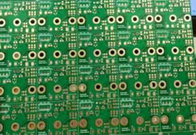
Controlled Depth Drilling is a precision drilling process used in PCB manufacturing to create holes that terminate at a predefined internal layer, rather than penetrating the entire board thickness. Unlike conventional through drilling, which passes from the top layer to the bottom layer, Controlled Depth Drilling allows the drill bit to stop accurately at a controlled depth measured in microns.
At its core, Controlled Depth Drilling is defined by depth accuracy, repeatability, and process control. The process relies on calibrated drilling machines, material stack-up data, and real-time feedback systems to ensure that each hole reaches its intended target layer without damaging adjacent copper foils or dielectric layers.
This capability is essential for forming:
Blind vias (outer layer to inner layer)
Back-drilled vias (removal of unused via stubs)
Sequential lamination interconnects
In modern high-layer-count PCBs, Controlled Depth Drilling is no longer an exception—it is a structural necessity.
To fully appreciate Controlled Depth Drilling, it is helpful to contrast it with traditional through-hole drilling.
Conventional drilling assumes uniform penetration through the entire PCB thickness. While this approach is simple and cost-effective, it introduces limitations such as:
Excessive via stubs
Signal reflection at high frequencies
Unnecessary layer-to-layer connections
Reduced routing density
Controlled Depth Drilling, by contrast, introduces intentional limitation. By stopping the drill at a defined depth, engineers can precisely control where electrical connections begin and end. This transforms vias from passive structures into engineered interconnect elements.
In my view, this distinction marks a philosophical shift: drilling is no longer just a mechanical operation—it becomes an electrical design tool.
Modern PCB architectures increasingly rely on:
HDI (High Density Interconnect) designs
Fine-pitch BGAs
High-speed serial interfaces
Mixed-signal and RF layouts
In these contexts, via stubs caused by full-depth drilling can significantly degrade signal integrity. Controlled Depth Drilling directly addresses this issue by eliminating unnecessary conductive paths.
Successful Controlled Depth Drilling begins long before the drill touches the panel. It starts at the stack-up design stage, where layer thicknesses, copper weights, and dielectric materials are carefully defined.
Designers must consider:
Target layer depth tolerance
Resin flow during lamination
Glass weave variation
Copper foil thickness accumulation
In my experience, Controlled Depth Drilling failures are rarely caused by drilling machines alone. They often originate from stack-up assumptions that ignore real manufacturing variation.
A well-designed stack-up allows drilling depth margins that are realistic rather than theoretical. This is where collaboration between designers and experienced fabricators—such as JM PCB—becomes critical, as manufacturing data can significantly improve design robustness.
Controlled Depth Drilling relies on multiple depth control mechanisms, including:
Z-axis servo calibration
Tool length measurement systems
Entry and backup material compensation
Depth offset programming
Each of these elements contributes to overall depth accuracy. However, no single mechanism is sufficient on its own. True process stability comes from system-level control, where machine calibration, material data, and process monitoring work together.
From a strategic perspective, this reinforces my belief that Controlled Depth Drilling is not easily commoditized. While many factories can claim the capability, only a subset can deliver it consistently at scale.
One of the most tangible benefits of Controlled Depth Drilling lies in signal integrity improvement. By eliminating via stubs, designers reduce:
Signal reflection
Impedance discontinuities
Crosstalk between layers
For high-speed digital signals, even a small unused via stub can behave like a resonant structure. Controlled Depth Drilling removes this risk at the source.
In RF and microwave designs, the impact is even more pronounced. Precise via termination ensures predictable impedance behavior, which simplifies simulation and improves first-pass design success.
Thermal cycling places significant stress on plated through holes. Longer vias experience greater differential expansion between copper and dielectric materials, increasing the likelihood of fatigue failure.
Controlled Depth Drilling mitigates this risk by reducing via length and mechanical leverage. As a result:
Copper barrel stress is lowered
Plating thickness distribution improves
Long-term reliability increases
This is a key reason why Controlled Depth Drilling is increasingly specified in automotive and aerospace standards, even when cost pressures remain high.
In high-density PCB design, space is no longer defined solely by board outline or layer count. Instead, vertical space inside the stack-up has become equally valuable. Controlled Depth Drilling directly addresses this hidden dimension by allowing engineers to selectively occupy only the electrical depth that is truly required.
From a strategic standpoint, this means that vias are no longer passive byproducts of routing—they become intentional structural elements. Designers can preserve inner-layer routing channels, reduce layer congestion, and delay or even avoid additional lamination cycles. Over large production volumes, this vertical efficiency translates into measurable cost savings and improved yield stability.
In my experience, many design teams initially adopt Controlled Depth Drilling to solve a single routing bottleneck, only to later realize that it fundamentally changes how they think about layer utilization.
One underestimated advantage of Controlled Depth Drilling is its influence on risk distribution across the manufacturing process. Traditional full-depth vias concentrate mechanical and thermal risk across the entire board thickness. Any plating weakness or micro-crack propagates through all layers.
By contrast, Controlled Depth Drilling localizes interconnections. Failures, if they occur, are confined to shorter structures with lower mechanical stress. This not only improves long-term reliability but also increases statistical yield consistency, particularly in complex HDI designs.
This is one reason why advanced fabrication partners such as JM PCB integrate Controlled Depth Drilling deeply into their process engineering philosophy, rather than treating it as a special request. Consistent depth control reduces variability, and reduced variability is the foundation of stable mass production.
No PCB material stack is perfectly uniform. Variations in dielectric thickness, resin content, and copper foil flatness all affect drilling depth accuracy. Controlled Depth Drilling magnifies these material realities because the acceptable tolerance window is significantly narrower than with through drilling.
Manufacturers must therefore compensate for:
Dielectric compression during lamination
Copper thickness accumulation across layers
Thermal expansion prior to drilling
In my view, the true difficulty of Controlled Depth Drilling lies not in the drilling itself, but in predicting how materials behave before the drill even starts.
Drill bit wear is a critical but often overlooked factor. Even minimal tool wear can shift actual drilling depth by several microns, which may be enough to damage target layers or leave residual stubs.
High-maturity Controlled Depth Drilling processes rely on:
Aggressive tool life tracking
Frequent depth recalibration
Conservative wear thresholds
This disciplined approach inevitably increases operational complexity, but it also explains why Controlled Depth Drilling cannot be executed reliably in low-control environments.
Every Controlled Depth Drilling operation exists within a narrow process window defined by:
Minimum penetration to ensure electrical connection
Maximum depth before damaging adjacent copper layers
Maintaining this window across thousands of panels requires more than equipment capability—it requires process culture. Documentation, feedback loops, and cross-department communication are essential.
This is where experienced suppliers differentiate themselves. In my observation, Controlled Depth Drilling succeeds most consistently in organizations that treat drilling as a system process, not a single machine step.
By reducing via length and eliminating unused stubs, Controlled Depth Drilling significantly improves electrical predictability. Impedance discontinuities are minimized, return paths are better controlled, and high-frequency losses are reduced.
For designers working with high-speed interfaces such as PCIe, Ethernet, or high-resolution sensor data lines, this improvement is not incremental—it is transformative. Controlled Depth Drilling allows simulations to align more closely with real-world measurements, reducing design iterations and time to market.
Shorter vias inherently experience less stress during thermal cycling. This improves resistance to:
Barrel cracking
Pad lifting
Interconnect fatigue
From a lifecycle perspective, Controlled Depth-Drilling extends product durability, especially in environments with frequent temperature fluctuations. This benefit often outweighs the initial process cost when evaluated across warranty cycles and field failure rates.
Controlled Depth Drilling is most justified when:
Via stubs exceed acceptable electrical length
Layer congestion limits routing completion
Reliability requirements exceed consumer-grade standards
However, I believe the decision should not be binary. Even partial adoption—targeting only the most critical signal layers—can deliver disproportionate benefits.
While Controlled Depth-Drilling adds upfront fabrication cost, this cost must be evaluated against:
Reduced layer count
Improved first-pass yield
Lower rework and failure rates
In practice, many designs achieve net cost neutrality or even cost reduction once these secondary effects are considered.
| Reliability Factor | Conventional Via Structure | Controlled Depth Drilling Structure |
|---|---|---|
| Thermal stress accumulation | High | Reduced |
| Barrel cracking risk | Elevated | Lower |
| Copper fatigue | More pronounced | Mitigated |
| Long-term stability | Dependent on margin | Inherently improved |
| Field failure probability | Higher | Lower |
Controlled Depth-Drilling represents a fundamental evolution in how vertical interconnections are conceived, designed, and manufactured. It transforms vias from unavoidable necessities into engineered structures that actively support performance, reliability, and space optimization.
The evolution of printed circuit board technology has always been driven by a single underlying tension: the need to pack more functionality into less space while maintaining long-term reliability. What distinguishes Controlled Depth-Drilling from many other manufacturing techniques is that it addresses this tension not by adding complexity for its own sake, but by introducing intentional control into a dimension that was once treated as fixed—the vertical structure of the PCB.
Throughout this article, Controlled Depth-Drilling has been examined not merely as a drilling method, but as a design-enabling strategy. By allowing interconnections to terminate precisely where they are needed, it fundamentally reshapes how designers think about layer utilization, signal behavior, and mechanical stress distribution. The resulting benefits—improved routing freedom, cleaner signal integrity, and enhanced reliability—are not isolated advantages. They reinforce one another across the entire product lifecycle.
From a manufacturing perspective, Controlled Depth-Drilling exposes an important truth: advanced PCB performance cannot be separated from process discipline. Depth accuracy, material predictability, and tool management are not optional refinements; they are prerequisites. This reality explains why Controlled Depth Drilling remains a differentiator among fabricators rather than a universally interchangeable capability. Consistent execution requires experience, data-driven control, and a conservative understanding of process limits.
Perhaps most importantly, Controlled Depth-Drilling encourages a shift in mindset. It challenges both designers and manufacturers to move away from default assumptions and toward deliberate structural decisions. Vias are no longer passive consequences of routing—they become engineered features whose length, position, and termination are chosen with intent. In high-speed, high-reliability, and high-density applications, this intentionality often marks the difference between marginal success and robust performance.
Looking forward, as signal speeds continue to rise and reliability expectations grow stricter, the strategic value of Controlled Depth-Drilling will only increase. Its role will extend beyond solving immediate technical problems and into shaping how future PCB architectures are conceived. Those who recognize it early—not as a cost factor, but as a system-level optimization tool—will be better positioned to unlock both space and reliability in the next generation of electronic products.
Designers should consider Controlled Depth Drilling at the stack-up planning stage, especially for HDI, high-speed, or high-reliability applications, where via behavior significantly influences performance.
Not necessarily. While it adds process steps, Controlled Depth Drilling can reduce overall cost by lowering layer count, improving yield, and reducing long-term failure rates.
By eliminating unnecessary via stubs, Controlled Depth-Drilling reduces impedance discontinuities and signal reflections, which is especially beneficial for high-speed designs.
In most low-layer-count designs, the benefits may be limited. However, it can still be valuable when specific signals require controlled impedance or enhanced reliability.
The primary risks involve depth accuracy and material variability. These risks are mitigated through precise calibration, conservative process windows, and experienced fabrication partners.


Connect to a Jerico Multilayer PCB engineer to support your project!
Request A Quote


 Quote
Quote