As printed circuit boards continue to evolve toward higher density, thinner geometries, and more aggressive electrical performance targets, many traditional assumptions in PCB fabrication are being quietly challenged. Processes and structures once considered secondary are now central to yield, reliability, and lifecycle performance. Among these, the Cap-Layer has emerged as a critical yet often underappreciated element in high-density PCB fabrication.
In advanced interconnect architectures—particularly those involving blind vias, buried vias, microvias, and sequential lamination—the Cap Layer plays a decisive role in defining mechanical integrity, electrical stability, and long-term reliability. Yet, despite its importance, it is frequently misunderstood, oversimplified, or treated as a passive material choice rather than a strategic design and process decision.

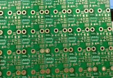
Cap Layer
The Cap-Layer refers to the conductive copper layer that seals, covers, or completes an interconnect structure—most commonly over vias, plated holes, or stacked microvia features—during PCB fabrication. It is not merely “another copper layer,” but a functional closure layer that finalizes the geometry and continuity of an interconnect path.
In high-density PCB fabrication, the Cap-Layer is typically formed after via formation and metallization. It may be created through panel plating, pattern plating, or copper filling followed by planarization, depending on the design and process flow. Its primary purpose is to ensure that the interconnect beneath it becomes electrically continuous, mechanically supported, and compatible with subsequent lamination or surface patterning steps.
What distinguishes the Cap-Layer from standard signal or plane layers is intent. While signal layers route current laterally, and plane layers distribute reference potential, the Cap Layer terminates and stabilizes vertical interconnects. It is, in essence, the structural “roof” of a via system.
Historically, the Cap Layer was little more than a byproduct of through-hole PCB manufacturing. Once holes were drilled and plated, outer copper layers naturally “capped” the via barrels. Reliability concerns were modest, interconnect densities were low, and mechanical stresses were forgiving.
The transition to HDI (High-Density Interconnect) technology radically changed this dynamic. Blind vias, buried vias, stacked microvias, and via-in-pad designs introduced vertical complexity that traditional via structures never faced. In these architectures, the Cap-Layer is no longer incidental—it is engineered.
Today’s Cap-Layer must account for:
Extremely thin dielectric separations
High aspect-ratio microvias
Copper filling quality and void control
Repeated thermal cycling during sequential lamination
Fine-line surface patterning above capped vias
This evolution has transformed the Cap-Layer into a reliability-critical interface, where poor design or process control can lead to latent failures rather than immediate defects.
At its core, the Cap-Layer serves three fundamental functions: electrical continuity, mechanical reinforcement, and process compatibility.
Electrically, the Cap-Layer completes the vertical current path. Any discontinuity, thinning, or defect at this interface increases local resistance and can become a hotspot under high current density or fast signal transitions.
Mechanically, the Cap-Layer distributes stress. During thermal expansion and contraction, vias act as stress concentrators. A well-formed Cap-Layer spreads these stresses into the surrounding copper and dielectric, reducing the likelihood of crack initiation.
From a process standpoint, the Cap-Layer provides a planar and stable surface for subsequent fabrication steps. Without it, lamination quality degrades, surface imaging becomes unreliable, and yield loss escalates rapidly.
The influence of the Cap-Layer on PCB electrical performance is often underestimated. While its thickness and geometry may seem minor compared to bulk copper planes, its position at interconnect junctions makes it disproportionately impactful.
In high-speed designs, even slight variations in Cap-Layer thickness can alter impedance continuity at via transitions. This can manifest as signal reflections, eye diagram degradation, or increased insertion loss—effects that are difficult to debug once the board is assembled.
In power delivery networks, insufficient Cap-Layer copper can raise via resistance, increasing IR drop and localized heating. Over time, this accelerates electromigration and degrades long-term reliability.
From an engineering perspective, treating the Cap-Layer as a controlled electrical element, rather than a fabrication artifact, is a necessary mindset shift for modern PCB design.
Mechanical reliability is where the Cap-Layer’s influence becomes most visible—often only after failure analysis.
Common failure modes associated with inadequate Cap-Layer design include:
Circumferential cracking at the via-cap interface
Copper thinning due to over-planarization
Delamination between cap copper and dielectric
Microvoid propagation under thermal cycling
These failures rarely occur in isolation. Instead, they reflect a system-level weakness, where Cap Layer thickness, copper grain structure, and adhesion quality interact with laminate CTE mismatch and assembly thermal profiles.
Effective Cap Layer design begins long before fabrication. It starts with intentional design rules that align electrical requirements with manufacturability.
Key design principles include:
Defining minimum Cap Layer thickness based on current density, not just plating capability
Avoiding excessive copper removal during planarization
Aligning via diameter, fill strategy, and cap thickness coherently
Considering sequential lamination thermal history when specifying cap copper
One of the most common design mistakes is assuming that “more copper is always better.” In reality, excessive Cap Layer thickness can introduce stress concentration and planarization challenges. Balance, not maximization, is the goal.
From a fabrication perspective, the Cap Layer is one of the most process-sensitive features on an HDI board. Achieving consistent results requires tight control over:
Plating chemistry and current distribution
Via filling uniformity
Mechanical or chemical planarization parameters
Copper adhesion and grain orientation
Small variations can cascade into large reliability risks. This is why advanced PCB suppliers invest heavily in statistical process control around Cap Layer formation.
No discussion of the Cap Layer is complete without addressing trade-offs. Thicker caps improve reliability but increase plating time and copper consumption. Tighter controls improve consistency but raise manufacturing cost.
The engineering challenge is to optimize, not over-engineer. In high-volume consumer electronics, the Cap Layer may be designed to meet minimum lifecycle requirements. In contrast, aerospace, medical, and industrial control applications demand conservative margins.
Understanding where a product falls on this spectrum is essential to making rational Cap Layer decisions.
As PCB technology continues to push boundaries, the Cap Layer is increasingly a differentiator rather than a commodity feature. Boards that survive harsh environments, aggressive thermal cycling, and long service lives often do so not because of exotic materials, but because of disciplined execution of fundamentals—and the Cap Layer is one of those fundamentals.
In my view, the industry’s growing focus on advanced simulation, digital twins, and AI-driven design will eventually extend to Cap Layer optimization. When that happens, we may finally stop treating it as invisible copper and start recognizing it as what it truly is: the foundation of reliable interconnects.
| PCB Structure Type | Cap Layer Primary Function | Key Reliability Contribution | Common Risks if Poorly Designed |
|---|---|---|---|
| Through-Hole PCB | Completes via barrel continuity | Maintains electrical integrity | Minor cracking under thermal stress |
| Blind Via PCB | Seals vertical interconnect | Prevents via-top cracking | Open circuits after reflow |
| Buried Via PCB | Structural reinforcement | Distributes internal stress | Delamination during lamination |
| Stacked Microvia PCB | Mechanical stabilization | Enhances fatigue resistance | Micro-cracks at via-cap interface |
| Via-in-Pad PCB | Surface planarity | Improves solder joint reliability | Solder voiding, pad collapse |
The Cap Layer is neither glamorous nor optional, yet it underpins nearly every aspect of high-density PCB reliability. From electrical integrity to mechanical endurance, from process stability to long-term performance, its influence is both subtle and profound.
In the pursuit of higher density, faster signals, and smaller form factors, PCB engineering has increasingly focused on visible innovations—finer traces, smaller vias, exotic materials, and advanced simulation tools. Yet, as this article has explored in depth, the long-term reliability of modern interconnect structures often depends on something far less visible: the Cap Layer.
The Cap Layer represents a convergence point where electrical design intent, material science, and manufacturing discipline intersect. It is neither a passive byproduct of plating nor a simple geometric closure. Instead, it is an engineered interface that determines how vertical interconnects behave under electrical load, thermal stress, mechanical fatigue, and time. When this interface is thoughtfully designed and rigorously controlled, it quietly enables stable performance across the entire lifecycle of the product. When it is overlooked, it becomes a latent risk that may only surface after deployment, when correction is no longer possible.
One of the most important insights to emerge from this discussion is that Cap Layer reliability cannot be achieved through isolated optimization. Thickness alone is not enough. Copper quality without adhesion control is insufficient. Process capability without design alignment is fragile. True robustness arises only when Cap Layer design, material selection, via strategy, and fabrication control are treated as a unified system rather than independent variables.
From a manufacturing perspective, the Cap Layer also serves as an honest indicator of process maturity. Consistent, defect-free cap formation is rarely accidental. It reflects disciplined chemistry control, stable plating systems, precise planarization, and a deep understanding of how small variations propagate into large reliability consequences. In this sense, evaluating Cap Layer capability provides valuable insight into a supplier’s engineering culture and long-term quality mindset.
Looking ahead, the importance of the Cap Layer is unlikely to diminish. As PCBs move toward even finer geometries, higher layer counts, and closer integration with advanced packaging technologies, the tolerance for interconnect weakness will continue to shrink. The Cap Layer will increasingly act as the structural and electrical bridge between traditional PCB fabrication and semiconductor-level interconnect expectations.
Ultimately, demystifying the Cap Layer is not about elevating a single process step—it is about embracing a broader engineering philosophy. Reliable systems are built not only through innovation, but through respect for foundational details. In high-density PCB fabrication, the Cap Layer embodies that principle. It is quiet, often overlooked, and absolutely essential.
By recognizing its true role and designing with intention rather than assumption, engineers and manufacturers can transform the Cap Layer from a hidden vulnerability into a deliberate strength—one that supports the next generation of reliable, high-performance electronic systems.
Because failures at the Cap-Layer interface often appear late in the product lifecycle. Proactive control reduces latent defects and improves long-term field reliability.
The Cap-Layer seals the microvia structure and distributes mechanical stress. Inadequate cap thickness or poor adhesion significantly increases the risk of cracking under thermal cycling.
No. While sufficient thickness is critical, excessive Cap-Layer copper can introduce stress concentration and planarization issues. Optimal thickness depends on current density, via geometry, and application requirements.
Surface AOI may miss subsurface Cap-Layer defects. Cross-section analysis, X-ray inspection, and reliability testing are often required for high-reliability applications.
Each lamination cycle introduces thermal stress. A well-designed Cap-Layer must withstand repeated expansion and contraction without cracking or delaminating.


Connect to a Jerico Multilayer PCB engineer to support your project!
Request A Quote


 Quote
Quote